Compensation circuit for input voltage offset of error amplifier and error amplifier circuit

Active Publication Date: 2018-07-03
ELITE SEMICON MEMORY TECH INC
View PDF5 Cites 0 Cited by
  • Summary
  • Abstract
  • Description
  • Claims
  • Application Information

AI Technical Summary

Benefits of technology

[0018]To sum up, the provided compensation circuit for the input voltage offset of the error amplifier can be designed easily and

Problems solved by technology

Unfortunately, the biasing current shifted with the process variation is not known

Method used


Image

  • Compensation circuit for input voltage offset of error amplifier and error amplifier circuit
  • Compensation circuit for input voltage offset of error amplifier and error amplifier circuit
  • Compensation circuit for input voltage offset of error amplifier and error amplifier circuit

Examples


Example

[0026]Reference will now be made in detail to the exemplary embodiments of the present disclosure, examples of which are illustrated in the accompanying drawings. Wherever possible, the same reference numbers are used in the drawings and the description to refer to the same or like parts.

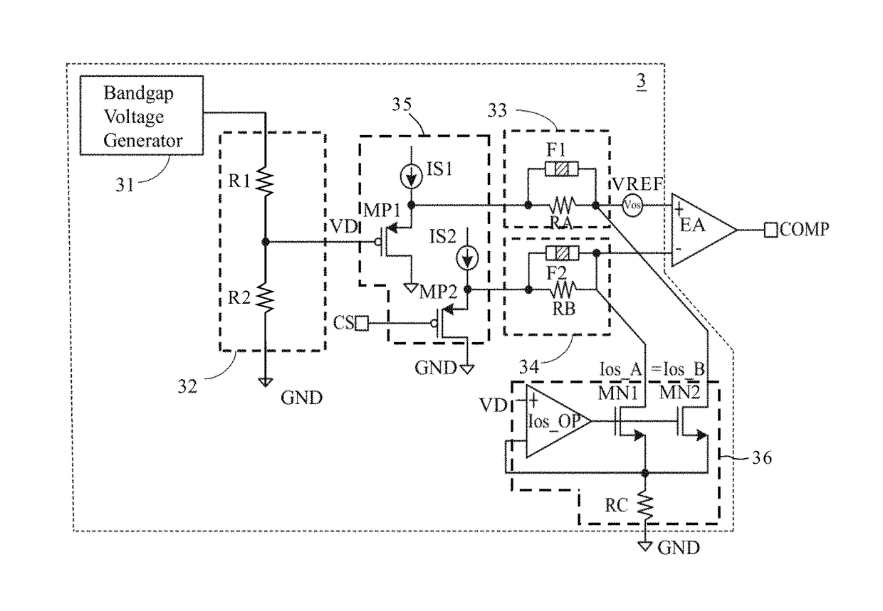
[0027]An exemplary embodiment of the present disclosure provides a compensation circuit used in an error amplifier circuit, and the compensation circuit can compensate the input voltage offset of the error amplifier in the error amplifier circuit. The compensation circuit compensates the input voltage offset in front of the input ends of the error amplifier, such that merely the input voltage offset should be measured in the circuit probing process. Then, the trimming code for input voltage offset can be calculated, wherein the trimming code records the ratio relation of the input voltage offset and resistance.

[0028]In the exemplary embodiment of the present disclosure, the resistors should be desig...


PUM


Abstract

A compensation circuit for compensating an input voltage offset of an error amplifier has a level shifter, a first trimming circuit, a second trimming circuit, and a compensation current sinking device. The level shifter shifts levels of a feedback voltage and a predetermined reference voltage and outputs a level shifted feedback voltage and a level shifted reference voltage. The first trimming circuit adjusts the level shifted reference voltage by trimming a first resistance thereof according to a trimming code, wherein the trimming code has the ratio relation of the input voltage offset and a resistance to be trimmed. The second trimming circuit adjusts the level shifted feedback voltage by trimming a second resistance thereof according to a trimming code. The compensation current sinking device sinks currents passing through the first and second trimming circuits.

Description

FIELD OF THE INVENTION[0001]The present disclosure relates to an error amplifier circuit, and in particular, to a compensation circuit for an input voltage offset of an error amplifier and an error amplifier circuit having the compensation circuit.BACKGROUND OF THE INVENTION[0002]The current marketed switching mode light emission diode (LED) driver is operated in a boundary current mode (BCM) and also has a closed loop circuit for locking a LED current. Referring to FIG. 1, FIG. 1A is a schematic diagram of a conventional switching mode LED driver. The conventional switching mode LED driver 1 comprises a current-to-voltage converter 11, an error amplifier EA, a compensation capacitor C_COMP, and a comparator CMP. The current-to-voltage converter 11 is connected to the error amplifier EA, and the error amplifier EA is connected to the compensation capacitor C_COMP and the comparator CMP.[0003]The LED current iLED (i.e. the current passing through the LED) is fed back to the switching...

Claims


Application Information

Patent Timeline
IPC IPC(8): H03K5/003H03K19/0185
CPCH03K5/003H03K19/018521H03F3/45475H03F3/45618H03F2203/45538H03F2203/45588
Inventor HO, I-HSIU
Owner ELITE SEMICON MEMORY TECH INC
Why Eureka
Try Eureka