
Semiconductor devices, a semiconductor diode and a method for forming a semiconductor device

a semiconductor diode and semiconductor technology, applied in the field of semiconductor device structure, can solve problems such as damage to components or devices, and achieve the effects of improving reverse recovery behavior, low switching current, and improving the handling of surge curren

Active Publication Date: 2018-07-31
INFINEON TECH AG
View PDF39 Cites 1 Cited by
  • Summary
  • Abstract
  • Description
  • Claims
  • Application Information

AI Technical Summary

Benefits of technology

This patent is about improving semiconductor devices by making them better at reversed recovery, reducing switching currents, and handling surge currents. The technical effects of this patent are to improve the performance and efficiency of semiconductor devices.

Problems solved by technology

Excess currents (or surge currents or over currents) in power semiconductor components or devices may be triggered by failures in supply networks (e.g. on the entry side of a converter or a phase short circuit), or in special conditions of an inverter load.
Power semiconductor components may be loaded with momentary or short term excess currents during operation, and may suffer from damages.

Method used


Image

  • Semiconductor devices, a semiconductor diode and a method for forming a semiconductor device
  • Semiconductor devices, a semiconductor diode and a method for forming a semiconductor device
  • Semiconductor devices, a semiconductor diode and a method for forming a semiconductor device

Examples


Embodiment Construction

[0026]Various example embodiments will now be described more fully with reference to the accompanying drawings in which some example embodiments are illustrated. In the figures, the thicknesses of lines, layers and / or regions may be exaggerated for clarity.

[0027]Accordingly, while example embodiments are capable of various modifications and alternative forms, embodiments thereof are shown by way of example in the figures and will herein be described in detail. It should be understood, however, that there is no intent to limit example embodiments to the particular forms disclosed, but on the contrary, example embodiments are to cover all modifications, equivalents, and alternatives falling within the scope of the disclosure. Like numbers refer to like or similar elements throughout the description of the figures.

[0028]It will be understood that when an element is referred to as being “connected” or “coupled” to another element, it can be directly connected or coupled to the other ele...


PUM


Abstract

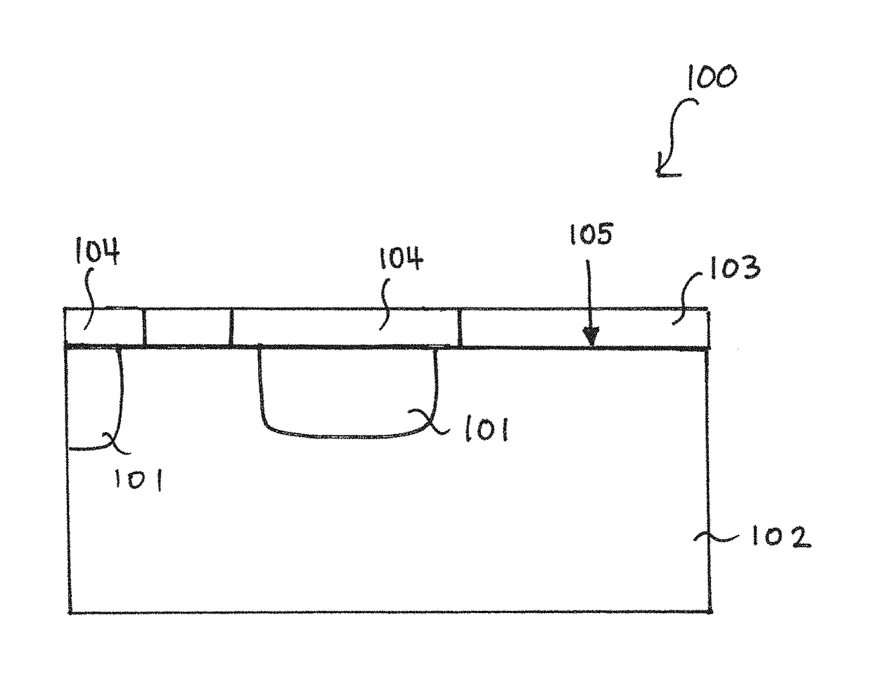
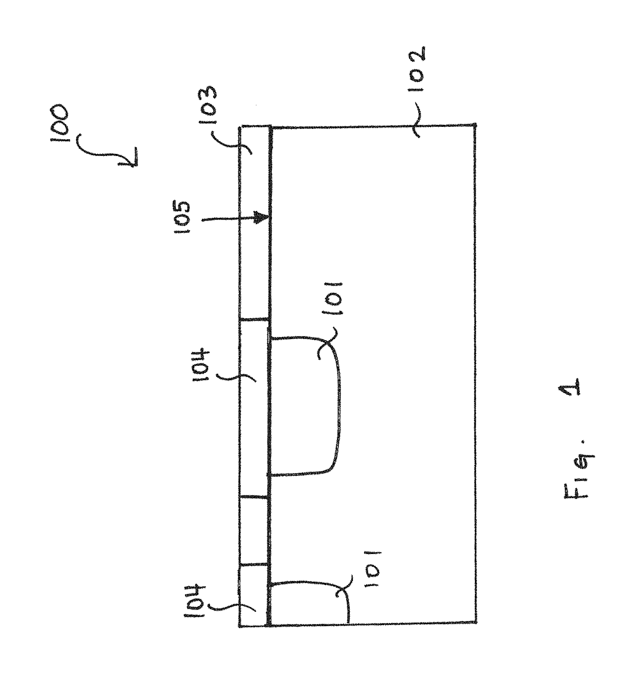
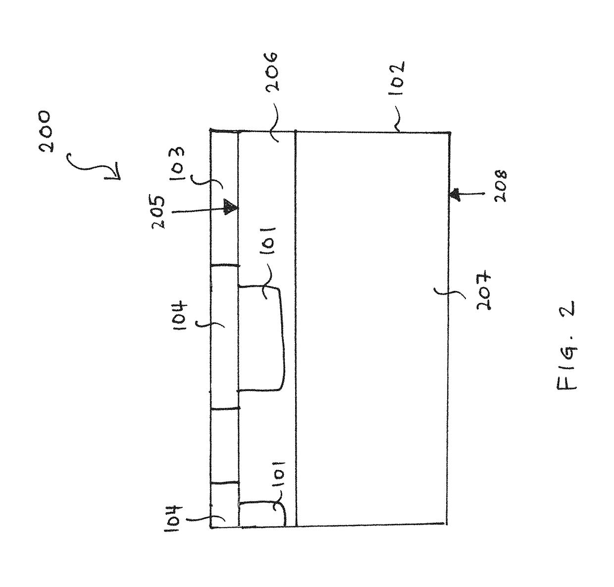
A semiconductor device includes at least one highly doped region of an electrical device arrangement formed in a semiconductor substrate and a contact structure including an NTC (negative temperature coefficient of resistance) portion arranged adjacent to the at least one highly doped region at a front side surface of the semiconductor substrate. The NTC portion includes a negative temperature coefficient of resistance material.

Description

TECHNICAL FIELD[0001]Embodiments relate to concepts for semiconductor device structures, and in particular to semiconductor devices, a semiconductor diode, and a method for forming a semiconductor device.BACKGROUND[0002]Excess currents (or surge currents or over currents) in power semiconductor components or devices may be triggered by failures in supply networks (e.g. on the entry side of a converter or a phase short circuit), or in special conditions of an inverter load. Power semiconductor components may be loaded with momentary or short term excess currents during operation, and may suffer from damages. It is desired to reduce damages caused by surge currents and improve the reliability of power semiconductor components when surge currents occur, for example.SUMMARY[0003]It is a demand to provide concepts for semiconductor devices with improved reverse recovery behavior, low switching currents and / or improved handling of surge currents.[0004]Some embodiments relate to a semicond...

Claims


Application Information

Patent Timeline
Patent Type & Authority Patents(United States)
IPC IPC(8): H01L29/861H01L29/47H01L29/45H01L29/06H01L29/08H01L29/36H01L29/16H01L29/872
CPCH01L29/861H01L29/0619H01L29/08H01L29/872H01L29/36H01L29/456H01L29/47H01L29/1608H01L29/7393
Inventor BASLER, THOMASMAHLER, JOACHIMSCHULZE, HANS-JOACHIM
Owner INFINEON TECH AG
Learn More