Reverse conducting semiconductor device and a fabrication method thereof

a semiconductor device and reverse conducting technology, applied in semiconductor devices, diodes, electrical devices, etc., can solve the problems of large radiator capacity, difficult to optimize diode characteristics independently, and degrade conversion efficiency, so as to achieve the effect of improving the reverse recovery characteristi

Active Publication Date: 2005-11-24
MITSUBISHI ELECTRIC CORP
View PDF4 Cites 109 Cited by
  • Summary
  • Abstract
  • Description
  • Claims
  • Application Information

AI Technical Summary

Benefits of technology

[0015] characterized in that a short lifetime region where a lifetime of the carrier is set shorter than the other portion of the first conductive type base layer is formed on a part of the first conductive type base layer.
[0016] The reverse conducting semiconductor device pertaining to the present invention with the above construction is a reverse conducting semiconductor device including an insulated gate bipolar transistors and a free wheeling diode which are formed on the substrate as a single piece and a short lifetime region is formed in the part of the first conductive type base layer; therefore, a quantity of carriers swept out from the first conductive type base layer during a recovery operation can be smaller, thereby enabling a reverse recovery characteristic to be improved.

Problems solved by technology

With such construction, the circuit requires a large capacity radiator and a conversion efficiency is also degraded, and since a thermal breakdown results due to rise in temperature of the transistors themselves according to a combination of an operating current and operating voltage, a resistance load circuit is not used in many of cases.
However, there have been problems that a conventional reverse conducting insulated gate bipolar transistor has an anode and cathode on the same plane, that current flow capabilities in both directions are not at the same level, that since an internal diode shares an element for constituting the insulated gate bipolar transistor, it is difficult to optimize a diode characteristic independently, and that especially a recovery characteristic of an internal diode is lower than that. of a diode in a case where an IGBT chip and a free wheeling diode chip are combined as a two-chip device.
Carriers accumulated in the junction end region located in the outer peripheral region of the chip cause current concentration in the boundary region with a cell portion while a recovery action works, resulting in another problem of breakdown of the chip.

Method used


Image

  • Reverse conducting semiconductor device and a fabrication method thereof
  • Reverse conducting semiconductor device and a fabrication method thereof
  • Reverse conducting semiconductor device and a fabrication method thereof

Examples


embodiment 1

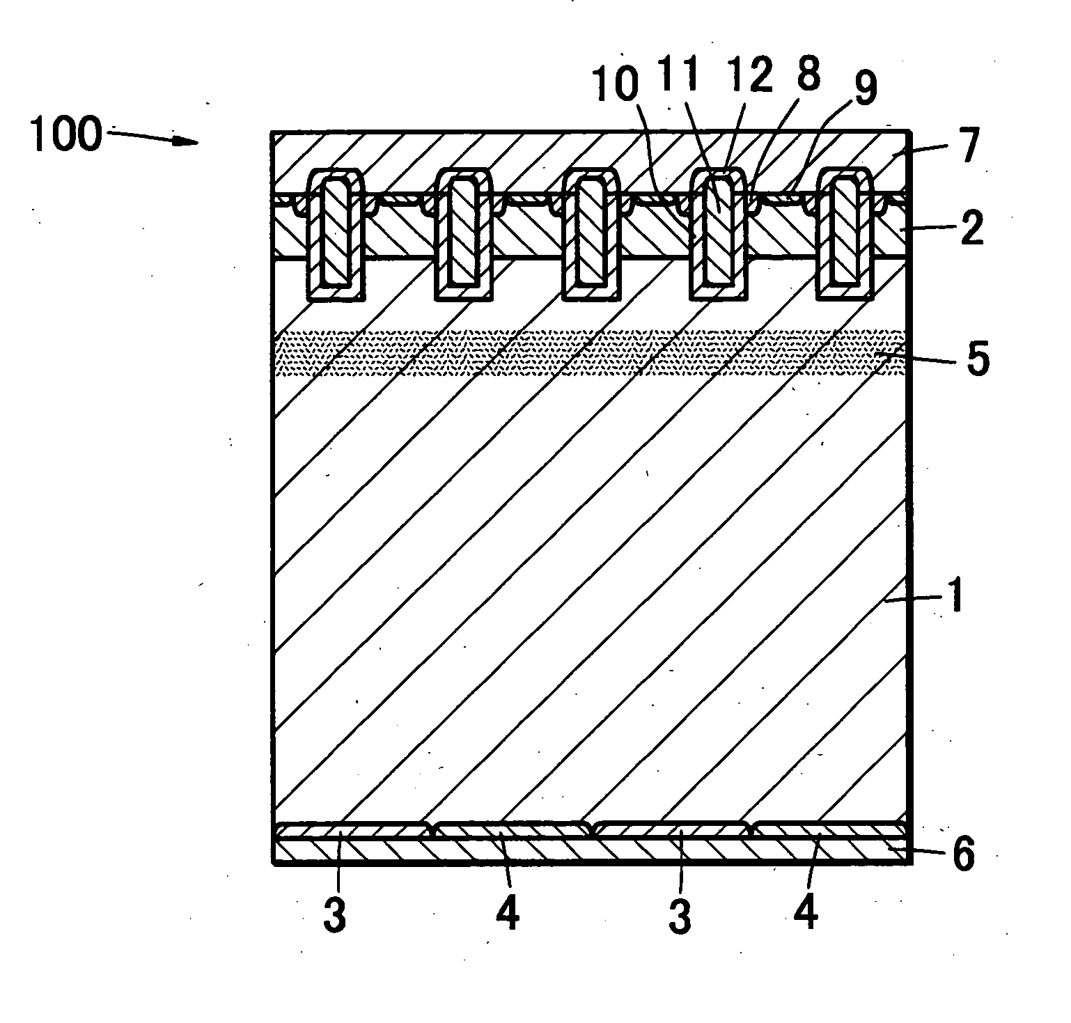
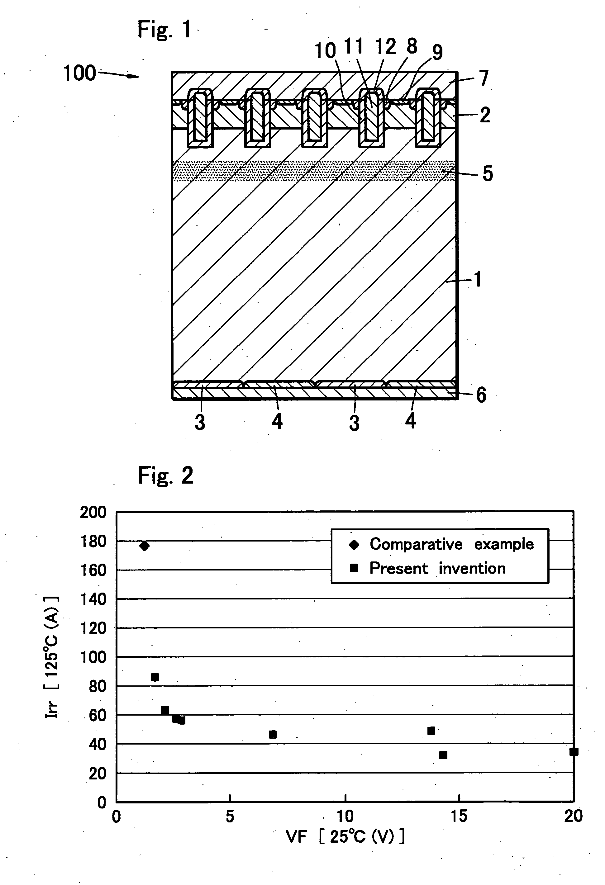
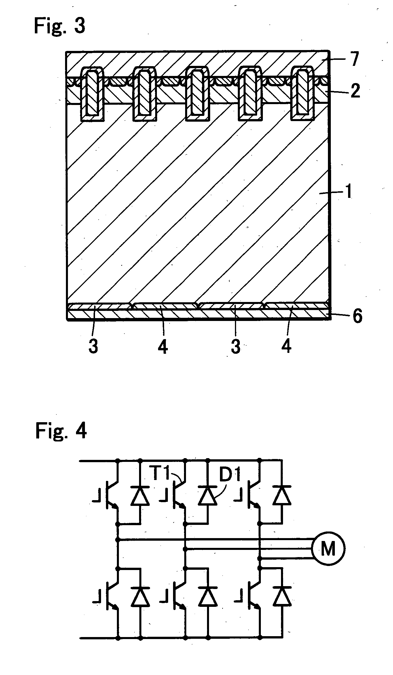
[0046] A reverse conducting semiconductor device of a first embodiment pertaining to the present invention includes insulated gate bipolar transistors and free wheeling diodes which are monolithically formed on a substrate 1 made of an N type semiconductor (for example, N type silicon semiconductor) as a single piece and is constructed in the following way (FIG. 1).

[0047] In a reverse conducting semiconductor device of the first embodiment, insulated gate bipolar transistors include:

[0048] (1) a P type base layer 2, (2) N+ emitter layers 8 formed by doping parts of the P type base layer 2 with an N type impurity, (3) P+type contact layers 9 formed on the P type base layer 2 between adjacent N+ emitter layers 8 by doping parts of the P type base layer 2 with a P type impurity, (4) gate insulating films 10 each formed so as to be in contact with the P type base layer 2, N+ emitter layers 8 and the N type semiconductor of the substrate 1, (5) gate electrodes 11 each formed so as to b...

embodiment 2

[0083] Description will be given of a reverse conducting semiconductor device of a second embodiment pertaining to the present invention below with reference to FIG. 14.

[0084] A reverse conducting semiconductor device of the second embodiment includes insulated gate bipolar transistors and free wheeling diodes are monolithically formed on a substrate 1 made of an N type semiconductor as a single piece and an electric field relaxation region 200 having a junction section end structure to relax an electric field in a peripheral portion during operation around an operating region 100 in which the insulated gate bipolar transistors and the free wheeling diodes formed as a single piece.

[0085] Note that since in the reverse conducting semiconductor device of the second embodiment, the operating region 100 is constructed in a similar way to that adopted in the first embodiment with the exception that no short lifetime region 5 is formed in the operating region 100, detailed description o...

embodiment 3

[0113] A reverse conducting semiconductor device of a third embodiment pertaining to the present invention is fabricated in a similar way to that adopted in the second embodiment with the exception that in the reverse conducting semiconductor device of the second embodiment, helium irradiation was further applied to form a short lifetime region 5, which is similar to that in the first embodiment (FIG. 27).

[0114] In order to confirm an effect of the reverse conducting semiconductor device of the third embodiment, a device of a 1200 V class was fabricated as a trial for evaluation. To be detailed, a thickness of the N type semiconductor layer is set to 190 μm and a region directly below of the junction section end structure is irradiated with an electron beam as lifetime control for all the N type semiconductor layer present in the electric field relaxation region and helium irradiation is applied in a similar way to that adopted in the first embodiment, in which case a recovery char...


PUM


Abstract

To provide a reverse conducting semiconductor device in which an insulated gate bipolar transistor and a free wheeling diode excellent in recovery characteristic are monolithically formed on a substrate, the free wheeling diode including; a second conductive type base layer to constitute the insulated gate bipolar transistor; a first conductive type base layer for constituting the insulated gate bipolar transistor, an anode electrode which is an emitter electrode covering a first conductive type emitter layer and the second conductive type base layer, a cathode electrode which is a collector electrode covering the first conductive type base layer and a second conductive type collector layer formed on the part of the first conductive type base layer, wherein a short lifetime region is formed on a part of the first conductive type base layer.

Description

BACKGROUND OF THE INVENTION [0001] 1. Field of the Invention [0002] The present invention relates to a reverse conducting semiconductor device in which an insulated gate bipolar transistor and a free wheeling diode are monolithically formed on a substrate as a single piece and a fabrication method thereof. [0003] 2. Description of the Background Art [0004] In recent years, inverter units have been widely used in home electric products, industrial power equipment and the like. An inverter unit is, since it usually employs a commercial power supply (an AC power supply), constituted of: a converter section conducting a forward conversion converting an AC power supply to a DC form once; a smoothing circuit section; and an inverter section inversely converting a DC voltage to an AC voltage. In the inverter section, insulated gate bipolar transistors capable of a high speed switching are mainly used as a main power device. In an inverter unit for power control, a current rating and voltag...

Claims


Application Information

Patent Timeline
Patent Type & Authority Applications(United States)
IPC IPC(8): H01L29/06H01L21/322H01L21/331H01L21/336H01L21/8234H01L27/04H01L27/06H01L27/088H01L29/08H01L29/739H01L29/76H01L29/78
CPCH01L21/263H01L29/7397H01L29/0834H01L29/86
Inventor AONO, SHINJIYAMAMOTO, AYATAKAHASHI, HIDEKIYAMAMOTO, KENZOYAMAMOTO, IKUKO
Owner MITSUBISHI ELECTRIC CORP
Why Eureka
Try Eureka