
Allocation of printed circuit boards on fitting lines

a technology of printed circuit boards and fitting lines, which is applied in the direction of electrical programme control, instruments, program control, etc., can solve the problems of not being able to produce every printed circuit board on every fitting, not exceeding the maximum production time capacity of the fitting line, and high utilization of one component of the fitting lin

Active Publication Date: 2018-08-28
SIEMENS AG
View PDF16 Cites 3 Cited by
  • Summary
  • Abstract
  • Description
  • Claims
  • Application Information

AI Technical Summary

Benefits of technology

[0014]More printed circuit boards than may be included in an equipment family may be allocated to a fitting line since the number of component types kept ready at the fitting line may not be arbitrary. The fitting line may occasionally be subjected to an equipment change, wherein the equipment for a first equipment family is exchanged for the equipment for a second equipment family. The less frequent the equipment changes and the fewer the component types exchanged during an equipment change, the more cost-effectively the fitting system may be operated.
[0025]In some embodiments, the allocation is carried out such that the sum of track consumptions of all components of a fitting line is minimized. Frequent changing of variable shuttle tables and the holding of a large number of shuttle tables may thus be avoided.

Problems solved by technology

However, for technical reasons, not every printed circuit board may be produced on every fitting line.
In addition, the maximum production time capacities of the fitting lines may not be exceeded.
In practice, unbalanced allocations are made repeatedly, thereby causing high utilization of one component of a fitting line and low utilization of another component.
As a result, the fitting system may not be optimally used.

Method used


Image

  • Allocation of printed circuit boards on fitting lines
  • Allocation of printed circuit boards on fitting lines
  • Allocation of printed circuit boards on fitting lines

Examples


Embodiment Construction

[0032]Linear optimization is used in the field of mathematical optimization for the optimization of linear target functions over a set that is restricted by linear equations and inequalities. Linear optimization is the basis of the solution methods of (mixed) integer linear optimization.

[0033]Advantages of linear optimization include that linear optimization is a global optimization approach and is readily expandable. In addition, there are very good commercial standard solvers (e.g., SCIP, CPLEX, Ilog, Xpress) that are widely available and reliable. An additional advantage of linear optimization is that for a determined solution, the maximum distance of the determined solution from the optimal solution (e.g., gap) is known.

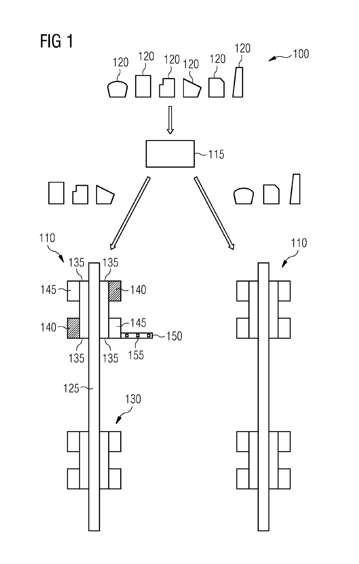
[0034]FIG. 1 shows a fitting system 100. The fitting system 100 includes a plurality of fitting lines 110 and a control device 115 configured for allocating printed circuit boards 120 to the fitting lines 110. Each fitting line 110 may include a transport system ...


PUM


Abstract

A method for allocating printed circuit boards to the fitting lines of a fitting system configured for fitting printed circuit boards with electronic components includes: determining requirements for fitting each of a plurality of printed circuit boards with respective components; and allocating the printed circuit boards to fitting lines under predetermined conditions by integral linear programming. The allocation is carried out such that differences between the component variances of the fitting lines are minimized. The component variance of a fitting line represent the number of different components configured to be fitted to all printed circuit boards allocated to the fitting line.

Description

RELATED APPLICATIONS[0001]This application is the National Stage of International Application No. PCT / EP2013 / 058527, filed Apr. 24, 2013, which claims the benefit of German Patent Application No. DE 102012211813.6, filed Jul. 6, 2012. The entire contents of both documents are hereby incorporated herein by reference.TECHNICAL FIELD[0002]The present teachings relate generally to a method for allocating printed circuit boards on fitting lines for fitting the printed circuit boards with components. The present teachings also relate to a control device for a production or assembly line for fitting printed circuit boards or other subassemblies with components. The present teachings also relate to a computer program product and a computer-readable medium.BACKGROUND[0003]In the field of electronics production, printed circuit boards or subassemblies may be produced on SMT fitting lines by surface mounting (e.g., surface mounted technology, SMT). However, for technical reasons, not every pri...

Claims


Application Information

Patent Timeline
Patent Type & Authority Patents(United States)
IPC IPC(8): G05B19/00G05B19/418H05K13/08
CPCG05B19/418H05K13/08G05B2219/45031H05K13/085
Inventor CRAIOVAN, DANIELHEROLD, NORBERTKEMPER, THORSTENPFAFFINGER, ALEXANDERROYER, CHRISTIAN
Owner SIEMENS AG
Learn More