Active faceted mirror system for lithography

a technology of lithography and faceted mirrors, applied in the field of lithography, can solve the problems of limited illumination system, limited illumination system, poor illumination effect, etc., and achieve the effects of cost saving, easy production of fields, and greater design flexibility and ease of us

Inactive Publication Date: 2006-05-18
ASML HLDG NV
View PDF17 Cites 68 Cited by
  • Summary
  • Abstract
  • Description
  • Claims
  • Application Information

AI Technical Summary

Benefits of technology

[0017] There are numerous benefits associated with the active faceted mirror system disclosed herein. In particular, the use of the active faceted mirror system allows greater design flexibility and ease of use in that illumination fields can be easily produced by electronically adjusting the...

Problems solved by technology

As the element or feature size (hereinafter referred to as “feature size”) desired to be imaged on the photosensitive substrate becomes smaller, technical problems often arise.
One of these problems is providing illumination, so that its image can be projected onto the photosensitive substrate.
Historically, there were few illumination systems that could provide the required illumination properties for projecting the image of the reticle or mask onto a photosensitive substrate at these operating wavelengths.
In some circumstances, these prior illumination systems may not provide the desired illumination and are relatively complicated.
Additionally, many of these systems are relat...

Method used


Image

  • Active faceted mirror system for lithography
  • Active faceted mirror system for lithography
  • Active faceted mirror system for lithography

Examples


Embodiment Construction

[0027] While the present invention is described herein with reference to illustrative embodiments for particular applications, it should be understood that the invention is not limited thereto. Those skilled in the art with access to the teachings provided herein will recognize additional modifications, applications, and embodiments within the scope thereof and additional fields in which the invention would be of significant utility.

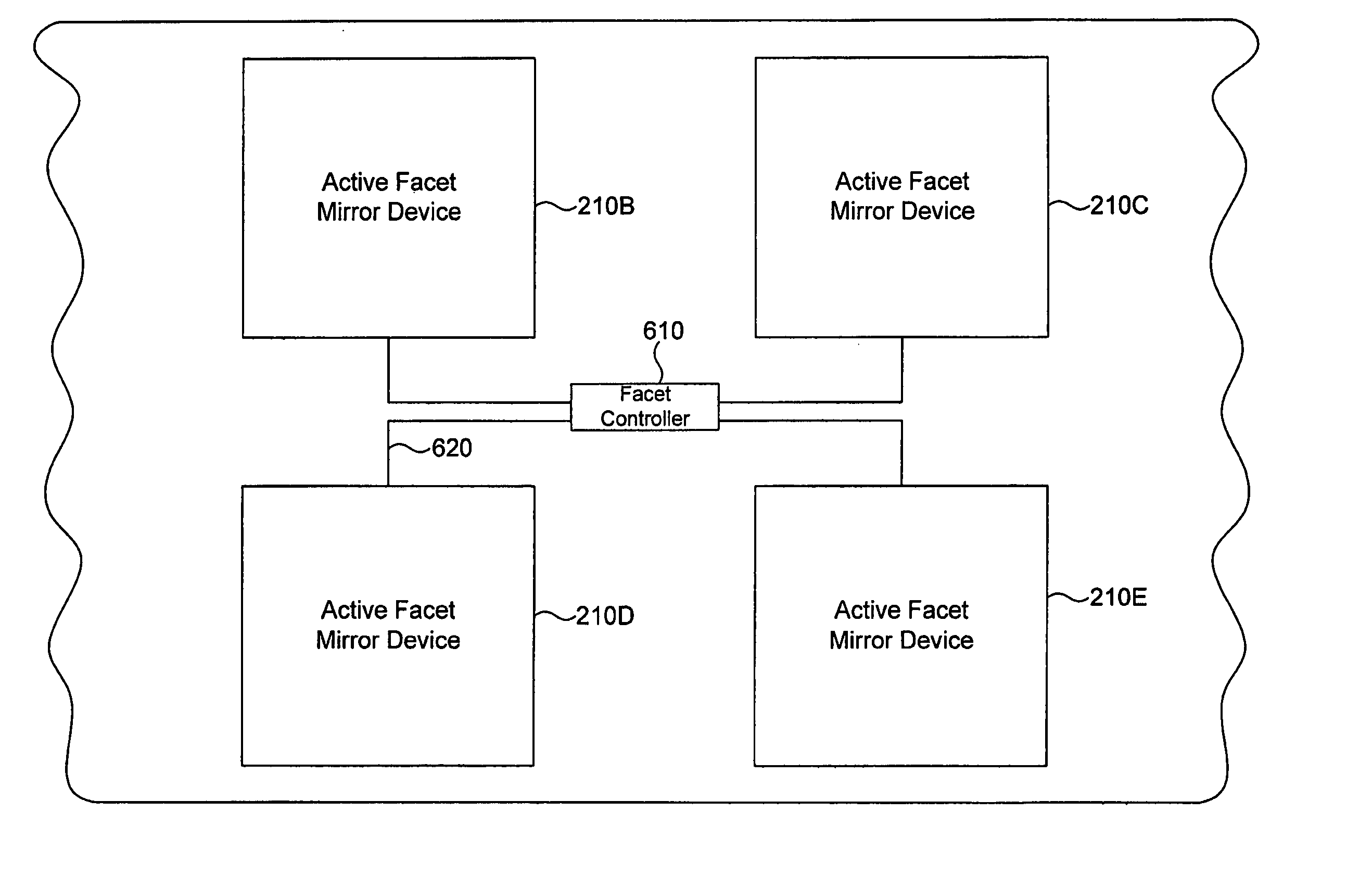
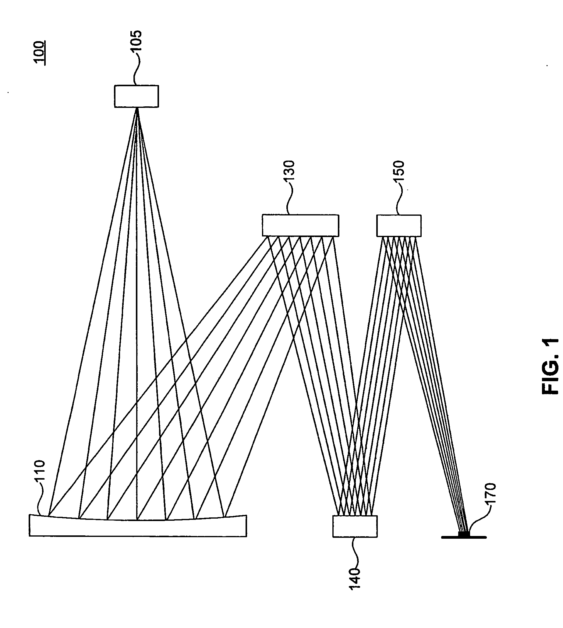
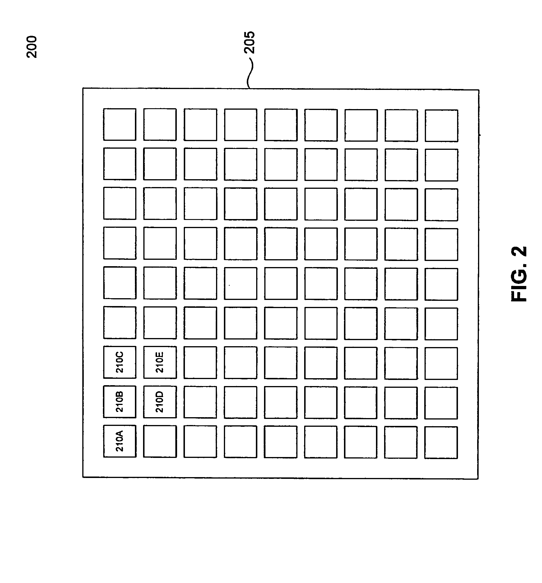
[0028]FIG. 1 illustrates illumination system 100 that uses fly's eye mirrors. Illumination system 100 includes illumination source 105, field facet mirror 110, pupil facet mirror 130, an optional first reflective element 140, and second reflective element 150.

[0029] Illumination source 105 can be a EUV source, such as a laser plasma source, a capillary discharge tube, or a synchrotron. Other types of light sources, including non-EUV sources can be used, as will be known by individuals skilled in the relevant arts. The electromagnetic radiation from ill...


PUM


Abstract

An active faceted mirror system is disclosed. The active faceted mirror system includes a set of active facet mirror devices, a base plate and a set of pins for mounting the active facet mirror devices to the base plate. Each of the active facet mirror devices includes a mirror substrate with a reflective surface and a bearing hole on the reverse side for mounting. Additionally, each of the active facet mirror devices includes at least three actuator targets located on the back side of the mirror substrate, a jewel bearing and a flexure for supporting the mirror substrate. The base plate includes a series of bearing holes for mounting the active facet mirror devices and at least three actuators for each of the active facet mirror devices. A set of facet controllers located on the base plate can be used to control the positioning of the active facet mirror devices to produce a desired illumination effect.

Description

BACKGROUND OF THE INVENTION [0001] 1. Field of the Invention [0002] The present invention relates to lithography, and more particularly, to an active faceted mirror system. [0003] 2. Background of Invention [0004] Lithography is often used in the manufacture of many devices and in particular, electronic and semiconductor devices, flat panel displays, print heads, micro / nano fluidic devices and the like. In a lithographic process, an image is projected onto a photosensitive substrate. As the element or feature size (hereinafter referred to as “feature size”) desired to be imaged on the photosensitive substrate becomes smaller, technical problems often arise. One of these problems is providing illumination, so that its image can be projected onto the photosensitive substrate. As the feature sizes of semiconductor devices becomes smaller, there is a need for photolithographic systems that provide a resolution of less than 0.065 micrometers. In order to achieve the imaging of these rela...

Claims


Application Information

Patent Timeline
IPC IPC(8): G02B26/00
CPCG02B7/1827G02B27/0905G02B27/0977G03F7/70116G03F7/702G03F7/70291
Inventor LOOPSTRA, ERIKROUX, STEPHEN
Owner ASML HLDG NV
Why Eureka
Try Eureka