Supercharge Your Innovation With Domain-Expert AI Agents!

Vertical transistor structure with looped channel

a transistor and looped channel technology, applied in the field of vertical fin field effect transistor (vertical finfet) device processing, can solve the problems of limiting the ability to use technical improvements designed for different transistor structures, imposing limitations on further improvement and/or integration into device structures with more complicated technical specifications

Active Publication Date: 2018-09-18
GLOBALFOUNDRIES US INC
View PDF6 Cites 2 Cited by
  • Summary
  • Abstract
  • Description
  • Claims
  • Application Information

AI Technical Summary

Benefits of technology

The patent describes a vertical FinFET structure that includes a looped channel region surrounded by a hollow interior. The structure includes a first source / drain region, a first gate, and a second source / drain region. The first gate is formed inside the looped channel region and includes a gate dielectric and a conductive gate region, while the second gate is formed outside the looped channel region. The second source / drain region is positioned on the upper surface of the looped channel region. This structure provides improved performance and stability of the FinFET device.

Problems solved by technology

In the case of a vertical FinFET, the conventional structure of a gate wrapping around a vertically-oriented semiconductor channel region may limit the ability to use technical improvements designed for different transistor structures.
The conventional vertical FinFET structure may also impose limitations on further improvement and / or integration into device structures with more complicated technical specifications, e.g., devices with increasingly high pattern densities.

Method used


Image

  • Vertical transistor structure with looped channel
  • Vertical transistor structure with looped channel
  • Vertical transistor structure with looped channel

Examples


Embodiment Construction

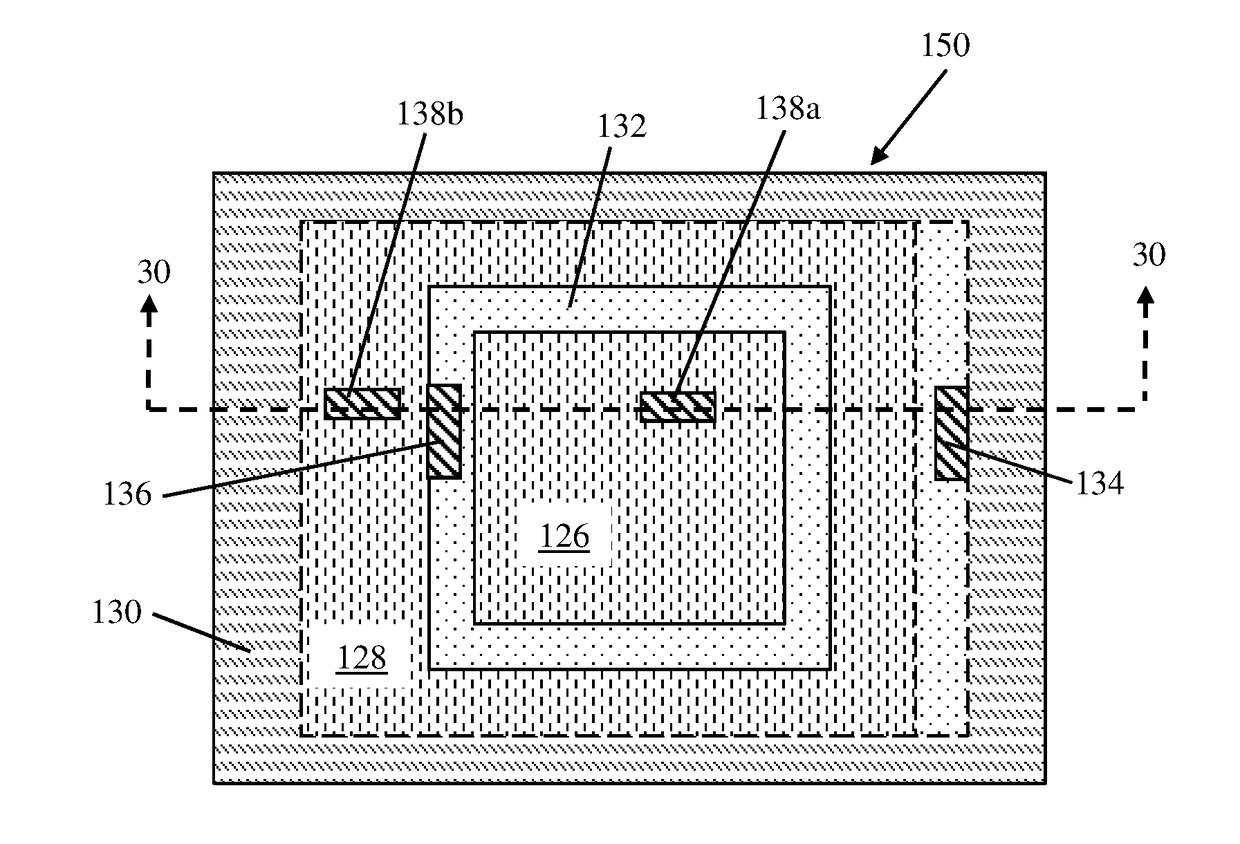
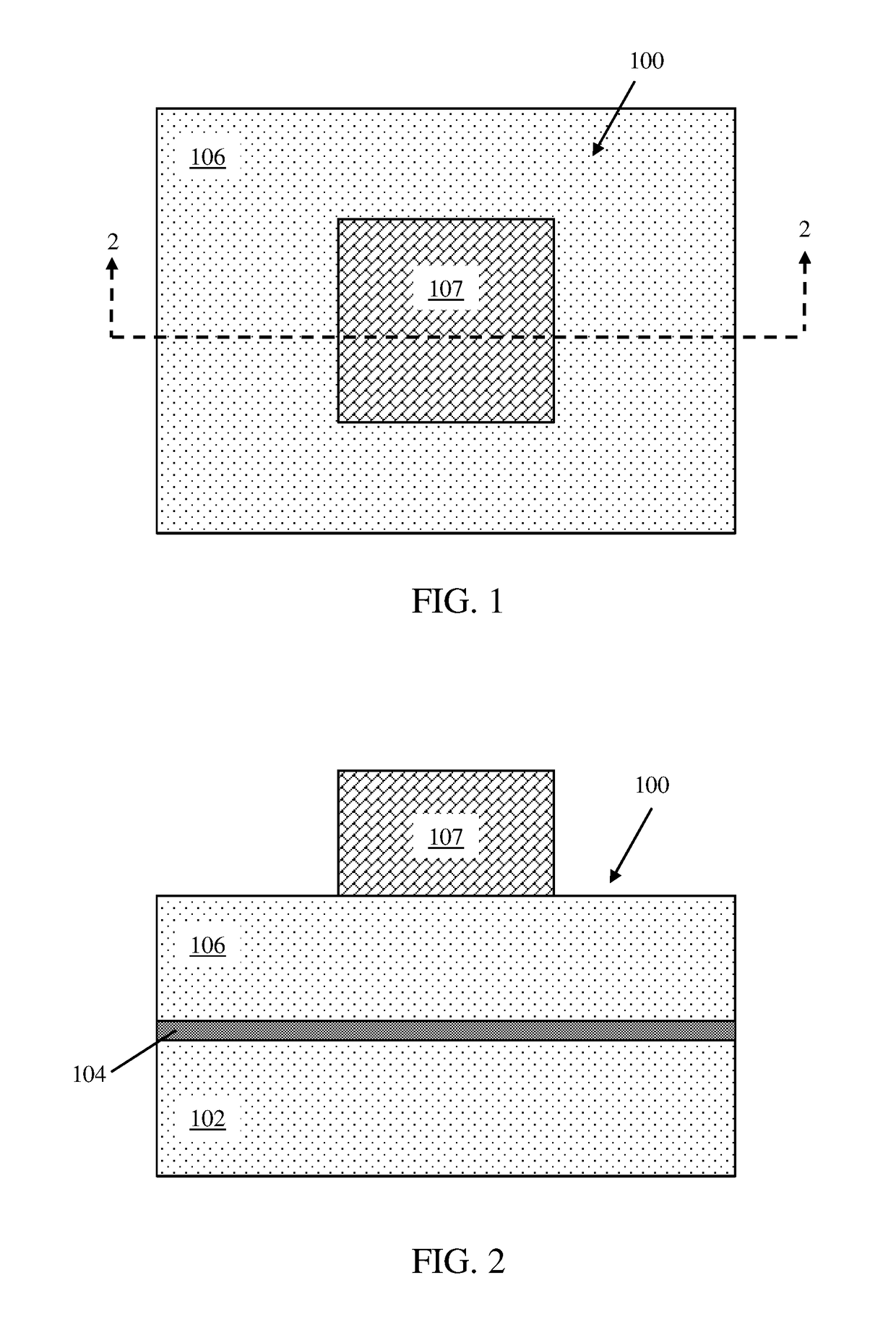
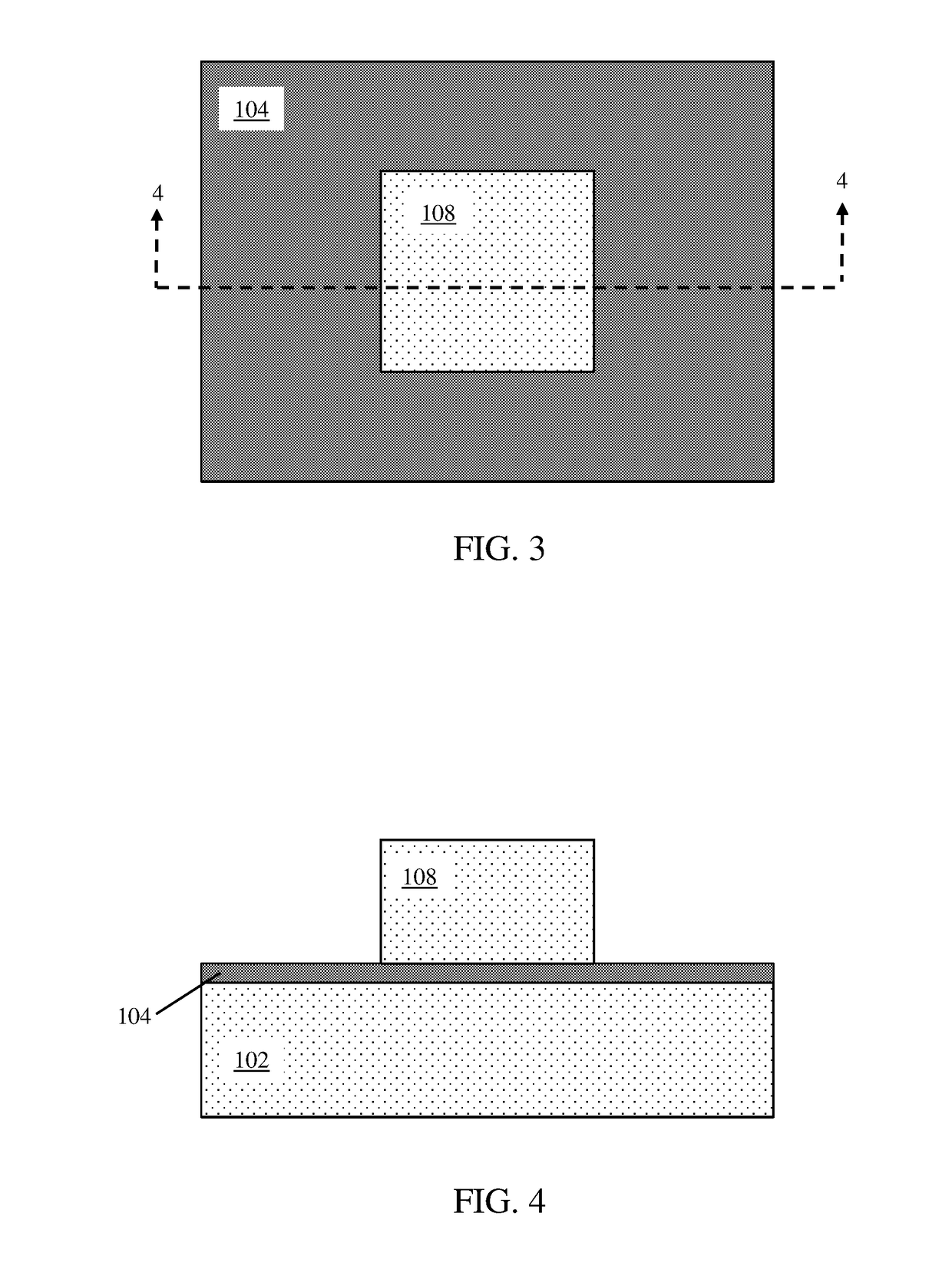
[0052]The disclosure provides a vertical fin-type field effect transistor (referred to herein as “vertical FinFET”) structure. Vertical transistors may be distinguished from other transistor configurations, e.g., MOSFET, FinFET, tunnel FET, and / or other types of transistors, by including a set of vertically stacked regions. For instance, a vertical transistor may include a source region positioned vertically beneath a gate region to the transistor, with an insulator vertically separating the gate from the source. Similarly, a drain region of the transistor may be positioned above and vertically separated from the gate region, e.g., with another insulating material. Contacts to the source, drain, and / or gate regions of a vertical transistor may be positioned laterally adjacent to the device in a shared dielectric layer in a spaced arrangement. Such vertical transistor structures are a contrast to other devices, e.g., where contacts to the various regions only extend vertically to the...


PUM


Abstract

The disclosure provides a vertical FinFET structure, including: a substrate including a first source / drain region; a looped channel region positioned on the first source / drain region of the substrate, the looped channel region having an inner perimeter which surrounds a hollow interior of the looped channel region; a first gate positioned within the hollow interior of the looped channel region, wherein the first gate is formed onto the looped channel region along the inner perimeter of the looped channel region; and a second source / drain region positioned on and overlying an upper surface of the looped channel region.

Description

BACKGROUNDTechnical Field[0001]The present disclosure relates to the processing of vertical fin field effect transistor (vertical FinFET) devices of an integrated circuit (IC) structure, and more particularly, to vertical FinFET structures which include a looped channel region.Related Art[0002]Advanced manufacturing of ICs requires formation of individual circuit elements, e.g., transistors such as field-effect-transistors (FETs) and the like, based on specific circuit designs. A FET generally includes source, drain, and gate regions. The gate region is placed between the source and drain regions and controls the current through a channel region (often shaped as a semiconductor fin) between the source and drain regions. Transistors may be formed over a substrate and may be electrically isolated with an insulating dielectric layer, e.g., inter-level dielectric (ILD) layer. Contacts may be formed to each of the source, drain, and gate regions through the dielectric layer in order to p...

Claims


Application Information

Patent Timeline
Patent Type & Authority Patents(United States)
IPC IPC(8): H01L21/70H01L21/768H01L21/8234H01L29/66H01L29/786
CPCH01L29/66666H01L29/78642H01L29/42392H01L21/76829H01L29/66643H01L29/66742H01L29/66833H01L21/823412
Inventor PANDEY, SHESH MANIZANG, HUIWATTS, JOSEF S.
Owner GLOBALFOUNDRIES US INC
Features
  • R&D
  • Intellectual Property
  • Life Sciences
  • Materials
  • Tech Scout
  • Unparalleled Data Quality
  • Higher Quality Content
  • 60% Fewer Hallucinations
Learn More