Radiation measuring apparatus and radiation measuring method

a radiation measurement and measuring device technology, applied in radiation measurement, instruments, measurement devices, etc., can solve the problems of difficult to realize a practical compton camera, low energy resolution of gas chamber detectors, and inability to realize a semiconductor detector using a compound camera

Active Publication Date: 2018-10-02
MITSUBISHI HEAVY IND LTD +2
View PDF16 Cites 0 Cited by
  • Summary
  • Abstract
  • Description
  • Claims
  • Application Information

AI Technical Summary

Problems solved by technology

However, the Compton camera using a semiconductor detector is not realized because a technique of confining the incidence direction of the electromagnetic radiation by using the recoiling direction of a recoil electron is generally not established in a practical form.
However, because a read time of data is very long in the CCD, the dead time becomes very large so that it is difficult to realize a practical Compton camera.
However, the gas chamber-type detector is low in the energy resolution, compared with the semiconductor detector.

Method used


Image

  • Radiation measuring apparatus and radiation measuring method
  • Radiation measuring apparatus and radiation measuring method
  • Radiation measuring apparatus and radiation measuring method

Examples


first embodiment

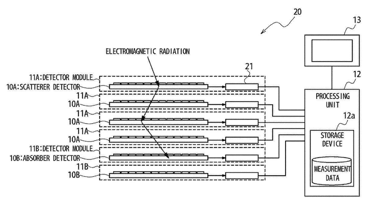
[0051]FIG. 4 is a block diagram showing an apparatus configuration of a Compton camera 20 in a first embodiment of the present invention. As shown in FIG. 4, the Compton camera 20 in the present embodiment includes a plurality of detector modules 11A and 11B, which are stacked, a processing unit 12 and a display device 13.

[0052]The detector module 11A is a module that includes a semiconductor detector functioning as a scatterer, and the detector module 11B is a module that includes a semiconductor detector functioning as an absorber. In the following description, the semiconductor detector functioning as the scatterer is called a scatterer detector 10A and the semiconductor detector functioning as the absorber is called an absorber detector 10B. The scatterer detector 10A and the absorber detector 10B are sometimes collectively called semiconductor detectors 10. The detector module 11A is located on the incidence side of electromagnetic radiation (e.g. gamma ray and X ray) to be mea...

second embodiment

[0081]In the Compton camera 20 of the first embodiment, a pixel-type detector is used that includes the pixel electrodes 2 arranged in a matrix as each scatterer detector 10A and each absorber detector 10B. One problem regarding the use of pixel-type detector is in that a quantity of data to be processed by the processing unit 12 increases when increasing the number of the pixel electrodes 2. When detecting the electromagnetic radiation by using the pixel-type detector, the data obtained from each pixel electrode must be processed. However, when tire number of the pixel electrodes increases, a quantity of data to be processed increases.

[0082]Especially, in the Compton camera 20 of the first embodiment, in order to specify the track of the recoil electron (the recoiling direction of the recoil electron), the spatial resolution of each scatterer detector 10A and each absorber detector 10B must be made high. For this purpose, the number of pixel electrodes 2 must be increased. To deal ...

third embodiment

[0119]In the second embodiment, the scatterer detector 10A is configured, to have the structure of the plurality of back electrodes 3 as shown in FIG. 11 to FIG. 16. However, in the Compton camera 20B of the third embodiment, the above-mentioned structure is adopted in which the plurality of back electrodes 3 are provided in the absorber detector 10B.

[0120]FIG. 21 is a block diagram of an example of configuration of the Compton camera 20B in the third embodiment. The configuration of Compton camera 20B in the third embodiment is similar to that of the Compton camera 20A in the second embodiment. However, in the Compton camera 20B of the third embodiment, the configuration of the detector module 11B loaded with the absorber detector 10B is changed to the configuration similar to the detector module 11A loaded with the scatterer detector 10A, following the change of the configuration of the absorber detector 10B.

[0121]FIG. 22 is a block diagram showing the configuration of detector mo...


PUM


Abstract

A radiation measuring apparatus (20) includes a scatterer detector (10A), an absorber detector (10B) and a processing unit (12). Pixel electrodes (2) of the scatterer detector (10A) and the absorber detector (10B) are arranged such that a distance between centers of two neighbor pixel electrodes (2) is smaller than a mean free path of a recoil electron generated in the Compton scattering of an electromagnetic radiation. The processing unit (12) specifies and incidence direction of the electromagnetic radiation based on a recoiling direction to which the recoil electron recoils. In this way, an electron tracking-type Compton camera is realized which confines the incidence direction of the electromagnetic radiation by using the recoiling direction of the recoil electron in a Compton camera using a semiconductor detector.

Description

TECHNICAL FIELD[0001]The present invention relates to a radiation measuring apparatus and a radiation measuring method, and especially, to a technique to detect an electromagnetic radiation such as X-ray and gamma ray by using a semiconductor detector.BACKGROUND ART[0002]A radiation measuring apparatus used to detect an electromagnetic radiation such as X-ray and gamma ray is sometimes configured to be able to specify an incidence direction of the electromagnetic radiation when an event has occurred in which the electromagnetic radiation is inputted to a detector of the radiation measuring apparatus. It becomes possible to specify a spatial distribution of radiation sources by specifying the incidence direction of the electromagnetic radiation. This is very useful in practical use.[0003]One of the radiation measuring apparatuses that are configured to specify the incidence direction of the electromagnetic radiation is a Compton camera. The Compton camera is a radiation measuring app...

Claims


Application Information

Patent Timeline
Patent Type & Authority Patents(United States)
IPC IPC(8): G01T1/29G01T1/24
CPCG01T1/241G01T1/2907G01T1/247G01T1/244G01T1/24G01T1/29
Inventor MATSUURA, DAISUKEKURODA, YOSHIKATSUGEMBA, KEITAKAHASHI, TADAYUKIWATANABE, SHINTAKEDA, SHIN'ICHIROYAMAMOTO, HIROOKOSUGI, KAZUMASAYAMAMURA, KAZUHISA
Owner MITSUBISHI HEAVY IND LTD
Why Eureka
Try Eureka