Field emission microelectronic device

a microelectronic device and field emission technology, applied in the direction of discharge tube/lamp details, electric discharge tubes, electrical apparatus, etc., can solve the problems of large bulk and weight of conventional vacuum tubes, unstable performance of transistors, and potential damage,

Inactive Publication Date: 2008-01-03
TSINGHUA UNIV +1
View PDF10 Cites 22 Cited by
  • Summary
  • Abstract
  • Description
  • Claims
  • Application Information

AI Technical Summary

Benefits of technology

[0010]In one embodiment, a nano-scaled field emission electronic device includes a substrate, a cathode electrode, and an anode electrode. The cathode electrode is placed on the substrate and has an emitter. The anode electrode is positioned opposite to and spaced from the cathode electrode. The nano-sc

Problems solved by technology

However, in some special applied fields, the vacuum tubes still have some superiorities that can not be replaced by the transistors.
Secondly, the performance of the transistors is mainly affected by the operating temperature thereof, thereby generally limiting the operating temperature to below 350° C. However, the performance of the vacuum tubes is, relatively, insensitive to the operating temperature thereof, allowing the vacuum tube to be stably operated at a relatively high temperature.
Thirdly, the performance of the transistors is greatly affected by the radiation of high-energy particles, with the performance of the transistors being unstable and even potentially damaged under a relatively large radiation intensity.
However, the performance of the vacuum tubes is basically insensitive to the radiation of high-energy particles, thereby permitting vacuum tube to be operated under a fairly sizable radiation intensity.
However, conventiona

Method used


Image

  • Field emission microelectronic device
  • Field emission microelectronic device
  • Field emission microelectronic device

Examples


first embodiment

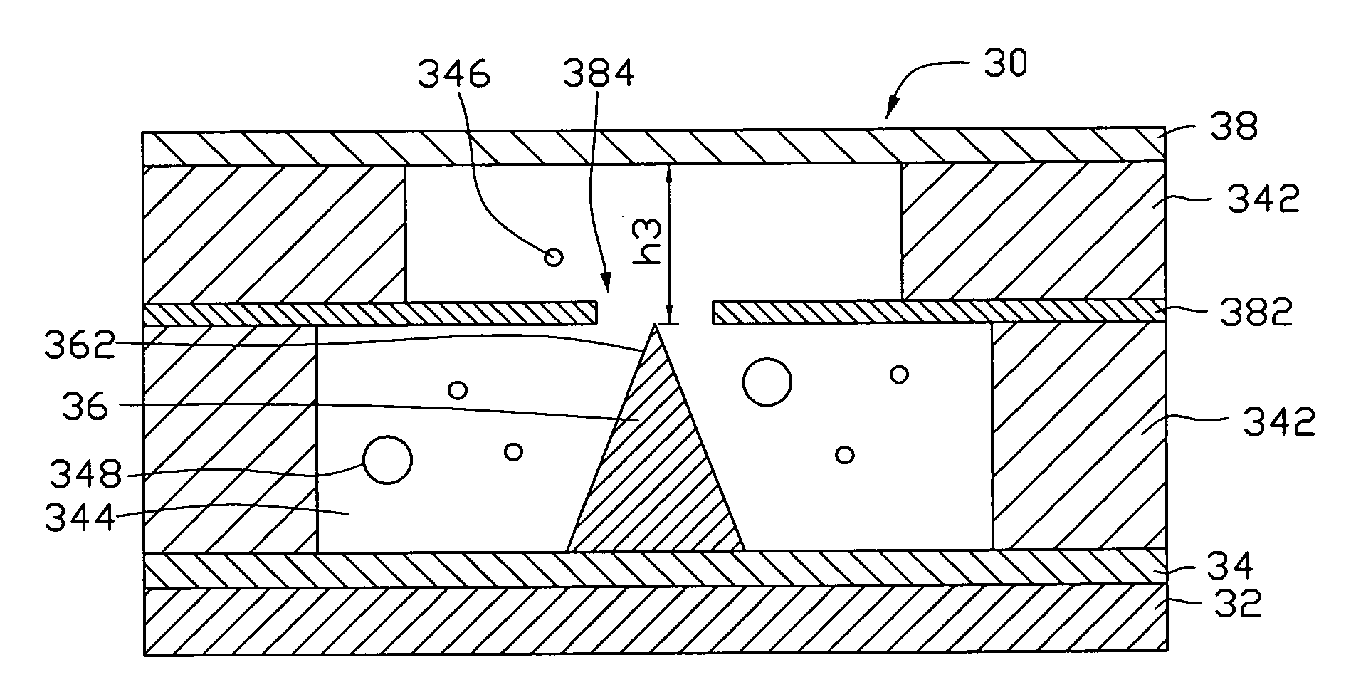
[0018]FIG. 1 shows a nano-scaled field emission electronic device 10, in accordance with the present device. As shown in FIG. 1, the nano-scaled field emission electronic device 10 is bipolar and includes a substrate 12, a cathode electrode 14, an emitter 16, and an anode electrode 18. The cathode electrode 14 is positioned on the substrate 12. The emitter 16 is located on and is electrically connected with the cathode electrode 14. The emitter 16 has an emission tip 162, and the emission tip 162 faces the anode electrode 18. A distance between the emission tip 162 of the emitter 16 and the anode electrode 18 is labeled as h1 and is named as a feature size (i.e., an emission distance) of the nano-scaled field emission electronic device 10. The anode electrode 18 is positioned apart from the cathode electrode 14, and an insulating layer 142 is located therebetween. This arrangement forms a sealed space 144 between the cathode electrode 14 and the anode electrode 18.

[0019]A plurality ...

second embodiment

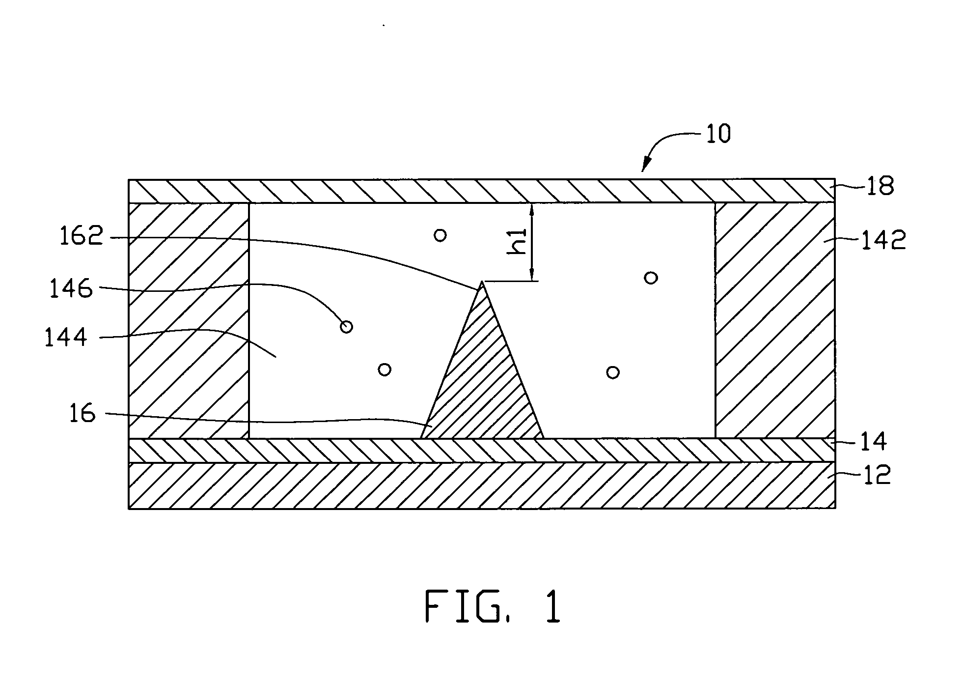
[0030]Referring to FIG. 2, a nano-scaled field emission electronic device 20, in accordance with the present device, is shown. The nano-scaled field emission electronic device 20 is a triode and includes a substrate 22, a cathode electrode 24, an emitter 26, an anode electrode 28, and a gate electrode 282. The cathode electrode 24 is positioned on the substrate 22. The emitter 26 is located on and electrically connected with the cathode electrode 24. The emitter 26 has an emission tip 262, and the emission tip 262 faces the anode electrode 28. The anode electrode 28 is positioned apart (i.e., spaced) from the cathode electrode 24, and the gate electrode 282 is located between the anode electrode 28 and the cathode electrode 24. An insulating layer 242 is located between the anode electrode 28 and the gate electrode 282 and between the gate electrode 282 and the cathode electrode 24. This arrangement forms a sealed space 244 between the cathode electrode 24 and the anode electrode 28...

third embodiment

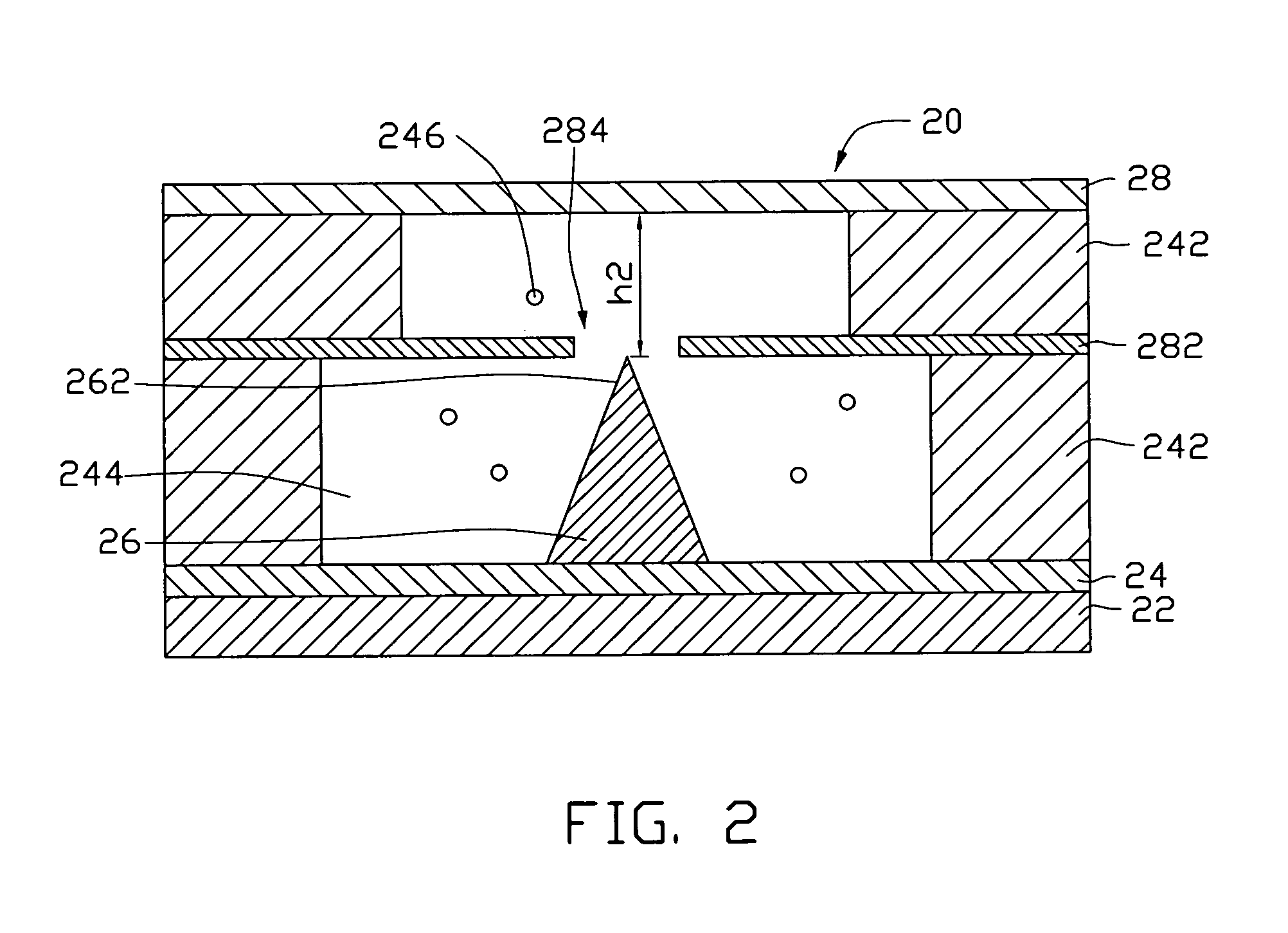
[0032]Referring to FIG. 3, a nano-scaled field emission electronic device 30, in accordance with the present device, is shown. The nano-scaled field emission electronic device 30 is a triode and includes a substrate 32, a cathode electrode 34, an emitter 36, an anode electrode 38, and a gate electrode 382. The cathode electrode 34 is positioned on the substrate 32. The emitter 36 is located on and is electrically connected with the cathode electrode 34. The emitter 36 has an emission tip 362, and the emission tip 362 faces the anode electrode 38. The anode electrode 38 is positioned apart from the cathode electrode 34, and the gate electrode 382 is located between the anode electrode 38 and the cathode electrode 34. An insulating layer 342 is located between the anode electrode38 and the gate electrode 382 and between the gate electrode 382 and the cathode electrode 34. This arrangement forms a sealed space 344 between the cathode electrode 34 and the anode electrode 38. A plurality...


PUM


Abstract

A nano-scaled field emission electronic device includes a substrate, a cathode electrode, and an anode electrode. The cathode electrode is placed on the substrate and has an emitter. The anode electrode is positioned opposite to and spaced from the cathode electrode. The nano-scaled field emission electronic device further has at least one kind of inert gas filled therein. The following condition is satisfied: h<λe, wherein h indicates a distance between a tip of the emitter and the anode electrode, and λe indicates an average free path of an electron in the inert gases. More advantageously, the following condition is satisfied:
h<λe_10.

Description

RELATED APPLICATIONS[0001]This application is related to commonly-assigned application entitled, “FIELD EMISSION MICROELECTRONIC DEVICE”, filed ______ (Atty. Docket No. US11438), the content of which is hereby incorporated by reference thereto.BACKGROUND[0002]1. Field of the Invention[0003]The invention relates generally to field emission microelectronic devices and, more particularly, to a nano-scaled field emission electronic device, which is operated in an inert gas environment.[0004]2. Discussion of Related Art[0005]The invention of computers is derived from vacuum tubes. The first computer in the world includes about 18,000 vacuum tubes. In 1947, transistors were invented by Bell laboratory. Due to the characteristic of a low energy consumption and cost, easy to be mini-sized and integrated, and suitability for mass production, transistors quickly replaced the vacuum tubes in most applied fields. This replacement made the invention of microprocessors and the mass use of compute...

Claims


Application Information

Patent Timeline
IPC IPC(8): H01J1/02
CPCH01J21/105H01J21/04
Inventor CHEN, PI-JINHU, ZHAO-FULIU, LIANGFAN, SHOU-SHAN
Owner TSINGHUA UNIV
Why Eureka
Try Eureka