Load port device and cleaning gas introducing method into a container on a load port

a technology of loading port and cleaning gas, which is applied in the direction of conveyors, electrical appliances, conveyor parts, etc., can solve the problems of contamination of the wafer surface before or after the processing to be housed in the container, and achieve the effects of bottom nozzles, reducing the number of introduction passages, and reducing the number of bottom holes

Active Publication Date: 2018-10-02
TDK CORPARATION
View PDF23 Cites 1 Cited by
  • Summary
  • Abstract
  • Description
  • Claims
  • Application Information

AI Technical Summary

Benefits of technology

[0007]As a result of miniaturization of semiconductor circuits, a higher cleanliness has been also recently demanded in the internal environment of the container housing the wafers so as to protect the wafer surfaces from oxidation and contamination. In the course of development for a load port maintaining a clean environment of the wafer container, it turned out that there is a problem that the wafer surface before or after processing to be housed in the container is contaminated by an outgas generated from the wafers soon after being processed, and that this contributes to prevention from improvement in quality.
[0008]The prevent invention has been achieved under such circumstances and provides a load port device and a cleaning gas introducing method into a container on the load port capable of maintaining a clean environment in a container and protecting a wafer surface from oxidation and contamination.

Problems solved by technology

In the course of development for a load port maintaining a clean environment of the wafer container, it turned out that there is a problem that the wafer surface before or after processing to be housed in the container is contaminated by an outgas generated from the wafers soon after being processed, and that this contributes to prevention from improvement in quality.

Method used


Image

  • Load port device and cleaning gas introducing method into a container on a load port
  • Load port device and cleaning gas introducing method into a container on a load port
  • Load port device and cleaning gas introducing method into a container on a load port

Examples


Embodiment Construction

[0034]Hereinafter, the present invention will be described based on embodiments shown in the figures.

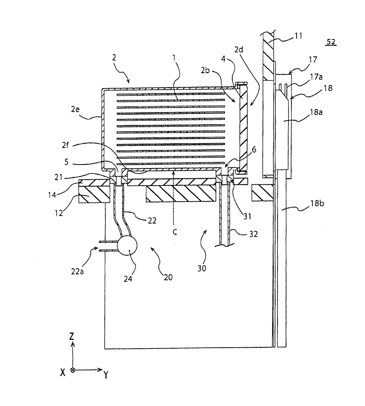
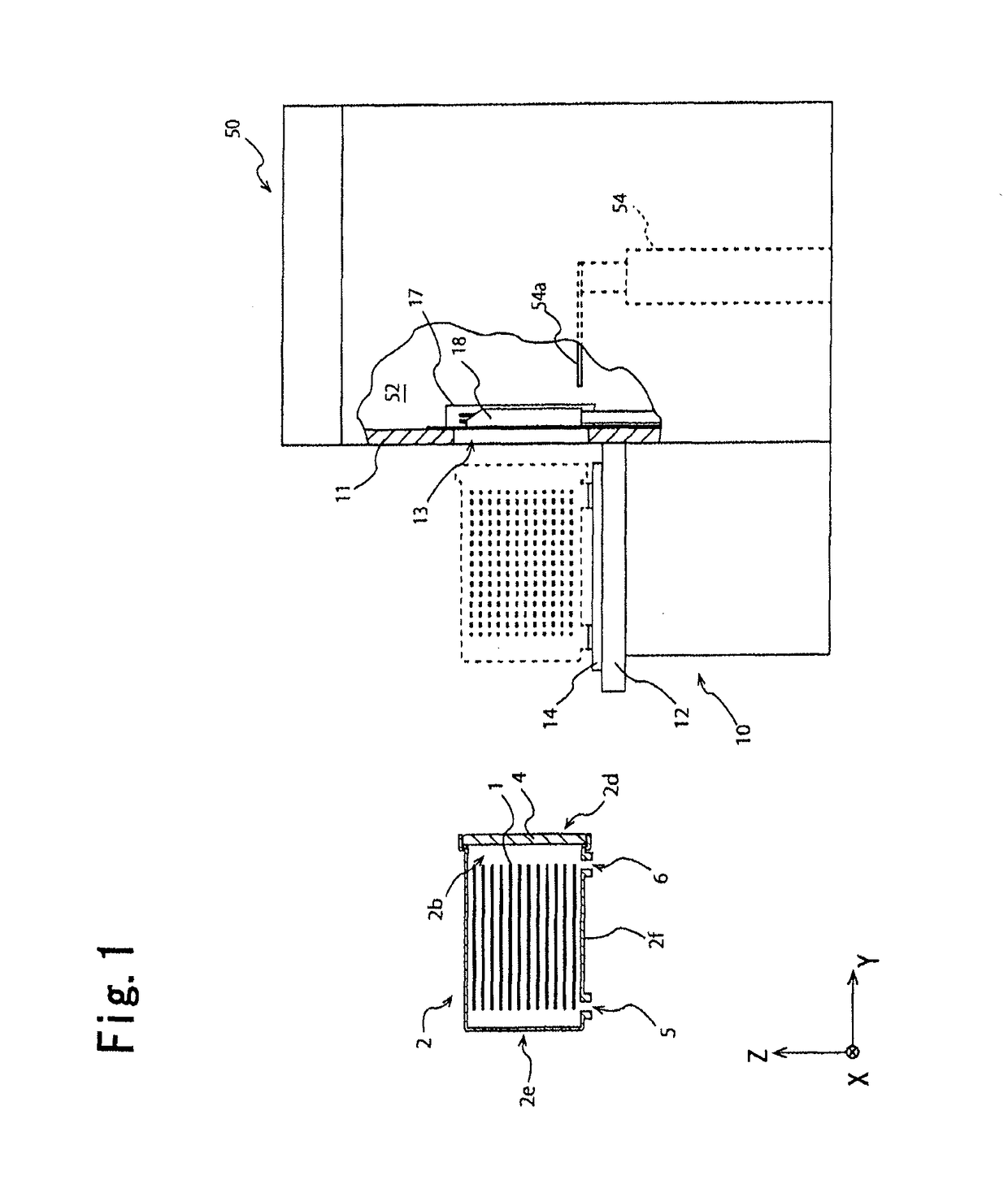
[0035]As shown in FIG. 1, a load port device 10 according to an embodiment of the present invention constitutes a part of an EFEM 50 of a front end module of a semiconductor processing apparatus. In addition to the load port device 10, the EFEM 50 has a minienvironment 52, a transportation robot 54, and the like. The minienvironment 52 is a space connecting a FOUP 2 as a container for transporting wafers 1 and a processing room (not shown). The transportation robot 54 is arranged in the minienvironment 52.

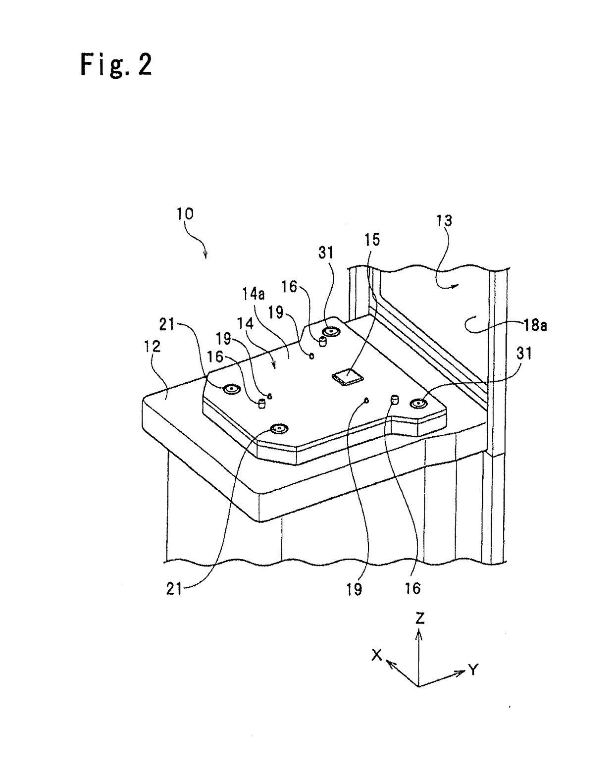
[0036]The load port device 10 has an installation stand 14 for installing the FOUP 2, an opening and closing part 18 for opening and closing the main opening 2b of the FOUP 2, and a front gas introduction part 17 for introducing a cleaning gas from the main opening 2b into the FOUP 2. As shown in FIG. 4, the load port device 10 has a gas discharge part 20 and a bottom gas introducti...


PUM


Abstract

A load port device includes an installation stand, an opening and closing part, a gas introduction part, and a gas discharge part. The installation stand installs a container whose side surface has a main opening for taking in and out a wafer. The opening and closing part opens and closes the main opening. The gas introduction part introduces a cleaning gas from the main opening into the container. The gas discharge part has a bottom nozzle capable of communicating with a bottom hole formed at a position distant from the main opening more than a bottom surface middle on a bottom surface of the container. The gas discharge part is capable of discharging a gas in the container to an outside of the container.

Description

BACKGROUND OF THE INVENTION[0001]1. Field of the Invention[0002]The present invention relates to a load port device where a container housing a wafer is installed at the time of processing the wafer and a cleaning gas introducing method into the container on the load port device.[0003]2. Description of the Related Art[0004]In manufacturing steps of semiconductors, wafers are transported between respective processing apparatuses using a container called a FOUP or so. When the wafers are processed, the container is installed on an installation stand of a load port device mounted on respective processing apparatuses, and the load port device communicates between a space in a transport container and a space in a processing room. This makes it possible to take out the wafers from the transport container using a robot arm or so and deliver the wafers to the processing room.[0005]In the environment of a container housing wafers, it is preferred to maintain an inactive state and a cleanline...

Claims


Application Information

Patent Timeline
Patent Type & Authority Patents(United States)
IPC IPC(8): H01L21/677H01L21/67H01L21/673H01L21/02
CPCH01L21/67766H01L21/02046H01L21/67017H01L21/67393H01L21/67772H01L21/67775H01L21/67353B65G2201/0297
Inventor OKABE, TSUTOMUOIKAWA, KOICHIRO
Owner TDK CORPARATION
Why Eureka
Try Eureka