Light emitting diode capable of generating different light colors over single wafer

a light-emitting diode and light-emitting diode technology, which is applied in the direction of basic electric elements, electrical appliances, semiconductor devices, etc., can solve the problems of reducing the utilization efficiency of light, and reducing the manufacturing cost.

Active Publication Date: 2018-10-09
EXCELLENCE OPTO INC
View PDF2 Cites 0 Cited by
  • Summary
  • Abstract
  • Description
  • Claims
  • Application Information

AI Technical Summary

Benefits of technology

[0010]To this end, the present invention is mainly intended to provide an LED capable of generating different light colors over a single wafer, which can adjust light intensities of different light colors as required and enables a color temperature of mixed light to meet demands in use.
[0013]Accordingly, in the present invention, a manner of providing the photo-luminescence material is adopted, and the at least two independently-distinguished light-emitting regions and the at least two independently-controlled circuit structures are cooperatively adopted, so light having two wavelengths may be emitted at least. Furthermore, by independently controlling the at least two circuit structures, light intensities of the light having two wavelengths can be further slightly adjusted to adjust color temperatures. Moreover, the circuit structures are provided on the single wafer substrate, processing and manufacturing can be completed at the same time, miniaturization can be achieved, manufacturing costs can be reduced, and demands in use can be met.

Problems solved by technology

But the prior art and structure will generate a large clearance between LEDs, thus being adverse to miniaturization.
When light having specific wavelength characteristics needs to be emitted, demands of light emission in different lighting occasions need to be met or a specific color for full-color display needs to be formed, in order to meet requirements for color accuracy, the earliest prior art refers to: binning many LED grains by utilizing spot measurement, sorting and binning programs to sort out LED grains close to the main wavelength distributions to result in considerable cost and time consumption of applications having different wavelength characteristic demands.
However, repeated wavelength conversion results in that the utilization efficiency of light is low, the phenomenon of high heat is easily caused, miniaturization is difficult to achieve and high-brightness demands cannot be met.
Moreover, a multi-layer stacking structure will increase manufacturing costs and reduce manufacturing yields, and demands in use are difficult to meet.

Method used


Image

  • Light emitting diode capable of generating different light colors over single wafer
  • Light emitting diode capable of generating different light colors over single wafer
  • Light emitting diode capable of generating different light colors over single wafer

Examples


Embodiment Construction

[0022]In order to make a member further understand and accept features, purposes and effects of the present invention, descriptions will be made with reference to a preferable embodiment and in conjunction with the drawings as follows.

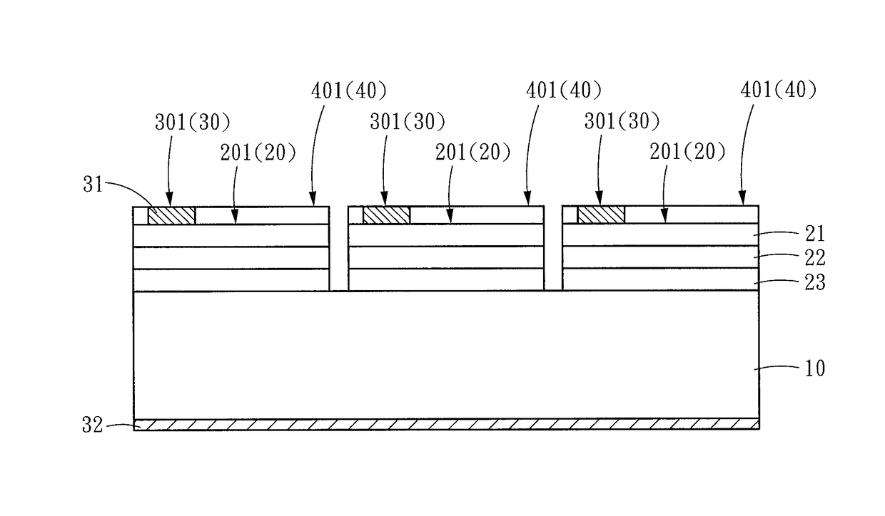
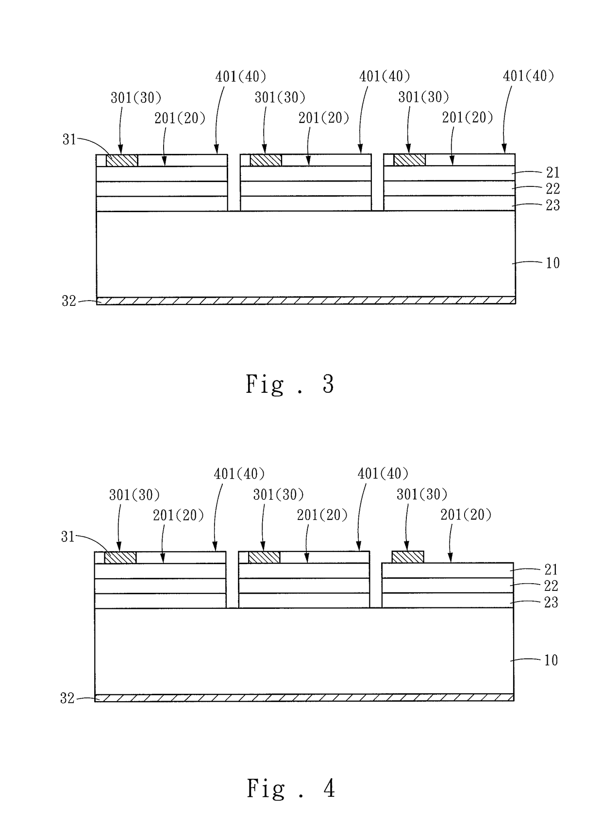
[0023]Referring to FIG. 3, FIG. 3 is an optical structure diagram of a first embodiment of the present invention. The structure is illustrated with a vertical-type LED. The structure is an LED light-emitting layer structure capable of generating different light colors over a single wafer, which comprises a wafer substrate 10, an LED light-emitting layer 20, a circuit layer 30 and an excitation material layer 40. In the present embodiment, the wafer substrate 10 is conductive and may adopt a silicon substrate.

[0024]The LED light-emitting layer 20 is provided on the wafer substrate 10, the LED light-emitting layer 20 includes at least two light-emitting regions 201, independently distinguished, and the LED light-emitting layer 20 may include a first-type...


PUM


Abstract

A wafer substrate, a light emitting diode (LED) light-emitting layer, a circuit layer and an excitation material layer are included. The LED light-emitting layer includes at least two light-emitting regions, independently distinguished. The circuit layer includes at least two circuit structures that correspond to the at least two light-emitting regions in quantity and are independently controlled. The excitation material layer includes at least one photo-luminescence material, at least one of the at least two light-emitting regions is provided with different photo-luminescence materials, and at least one of the at least two light-emitting regions is not provided with the photo-luminescence material. Accordingly, in the present invention, at least two light colors can be formed over a single wafer substrate through the at least two independently-controlled circuit structures and providing the different photo-luminescence materials.

Description

FIELD OF THE INVENTION[0001]The present invention relates to a light source structure of a light emitting diode (LED), and more particularly to an LED structure capable of generating different light colors over a single wafer.BACKGROUND OF THE INVENTION[0002]A light emitting diode (LED) is a luminescence assembly. A luminescence principle thereof is to exert a forward bias voltage (current) on a III-V compound semiconductor material, and to utilize a form of combining electrons and electron holes in the LED with each other and converting energy into light, where light can be emitted during energy release and the LED will not be as hot as an incandescent lamp bulb after being used for a long time. The LED is advantageous in small size, long life, low drive voltage, high response rate and excellent seismic resistance, can meet demands for various lightweight, thin and miniaturized devices, and has become a product popularized in daily life.[0003]Referring to FIG. 1 and FIG. 2, LEDs ma...

Claims


Application Information

Patent Timeline
Patent Type & Authority Patents(United States)
IPC IPC(8): H01L33/08H01L33/50H01L33/00H01L33/48
CPCH01L33/08H01L33/50H01L33/0079H01L33/48H01L25/0753H01L33/504
Inventor HUANG, KUO-HSINWU, CHUN-DERTSAI, TZENG-GUANGTSENG, KUO-SHU
Owner EXCELLENCE OPTO INC
Why Eureka
Try Eureka