Supercharge Your Innovation With Domain-Expert AI Agents!

Antenna device having patch antenna

a technology of patch antenna and antenna, which is applied in the direction of antenna coupling, antenna earthing, antenna, etc., can solve the problems of affecting radiation from the end portions, and affecting the performance of the patch antenna, so as to reduce the fluctuations in the operating frequency of the conductive structure due to the tolerance of the connection conductor, and reduce the disturbance of the directivity of the patch antenna

Active Publication Date: 2018-12-11
DENSO CORP
View PDF6 Cites 0 Cited by
  • Summary
  • Abstract
  • Description
  • Claims
  • Application Information

AI Technical Summary

Benefits of technology

The solution effectively reduces unwanted radiation and maintains directivity stability by minimizing frequency fluctuations, ensuring consistent performance despite tolerance variations in the connection conductor dimensions.

Problems solved by technology

Radiation from the substrate end portions due to this surface current is unnecessary radiation that adversely affects the performance of the patch antenna.
In other words, radiation from the end portions disturbs the directivity of the patch antenna.

Method used


Image

  • Antenna device having patch antenna
  • Antenna device having patch antenna
  • Antenna device having patch antenna

Examples


first embodiment

[0036][First Embodiment]

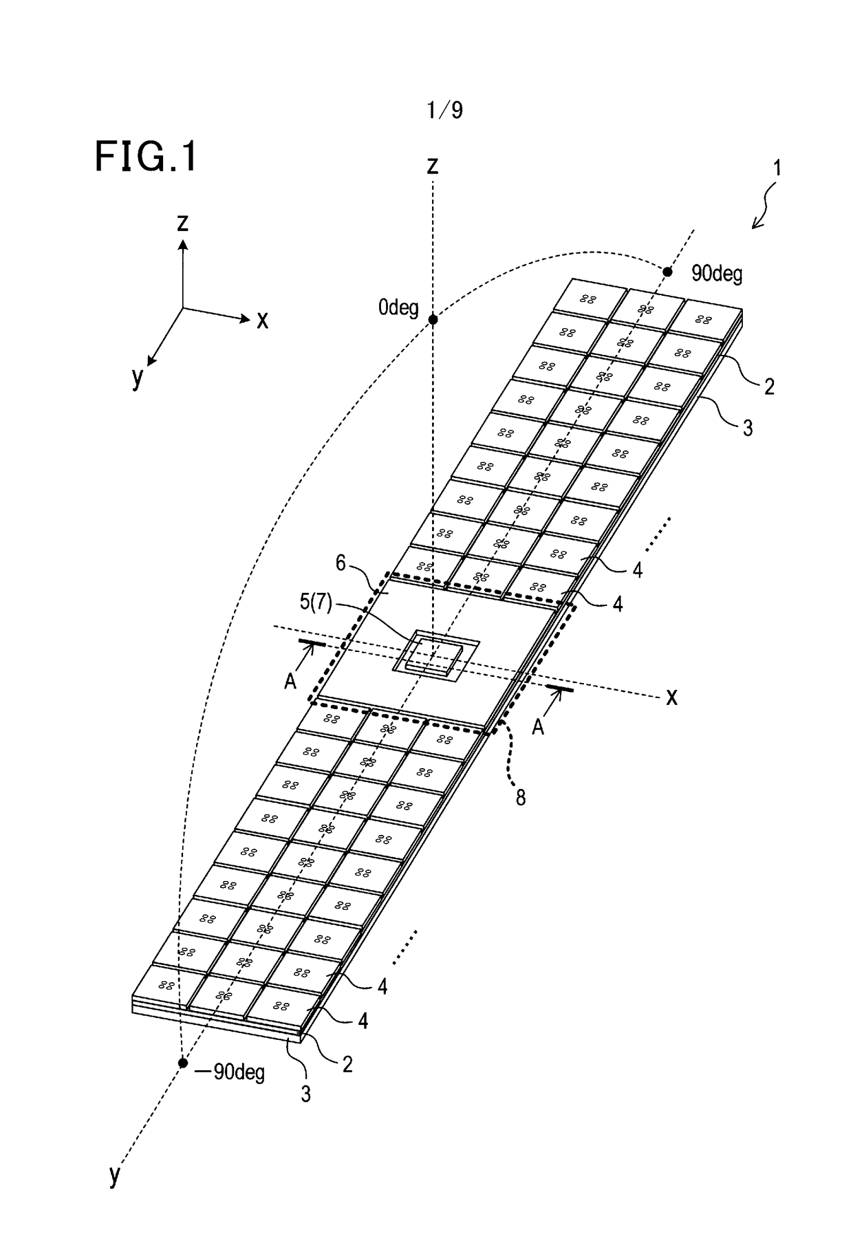
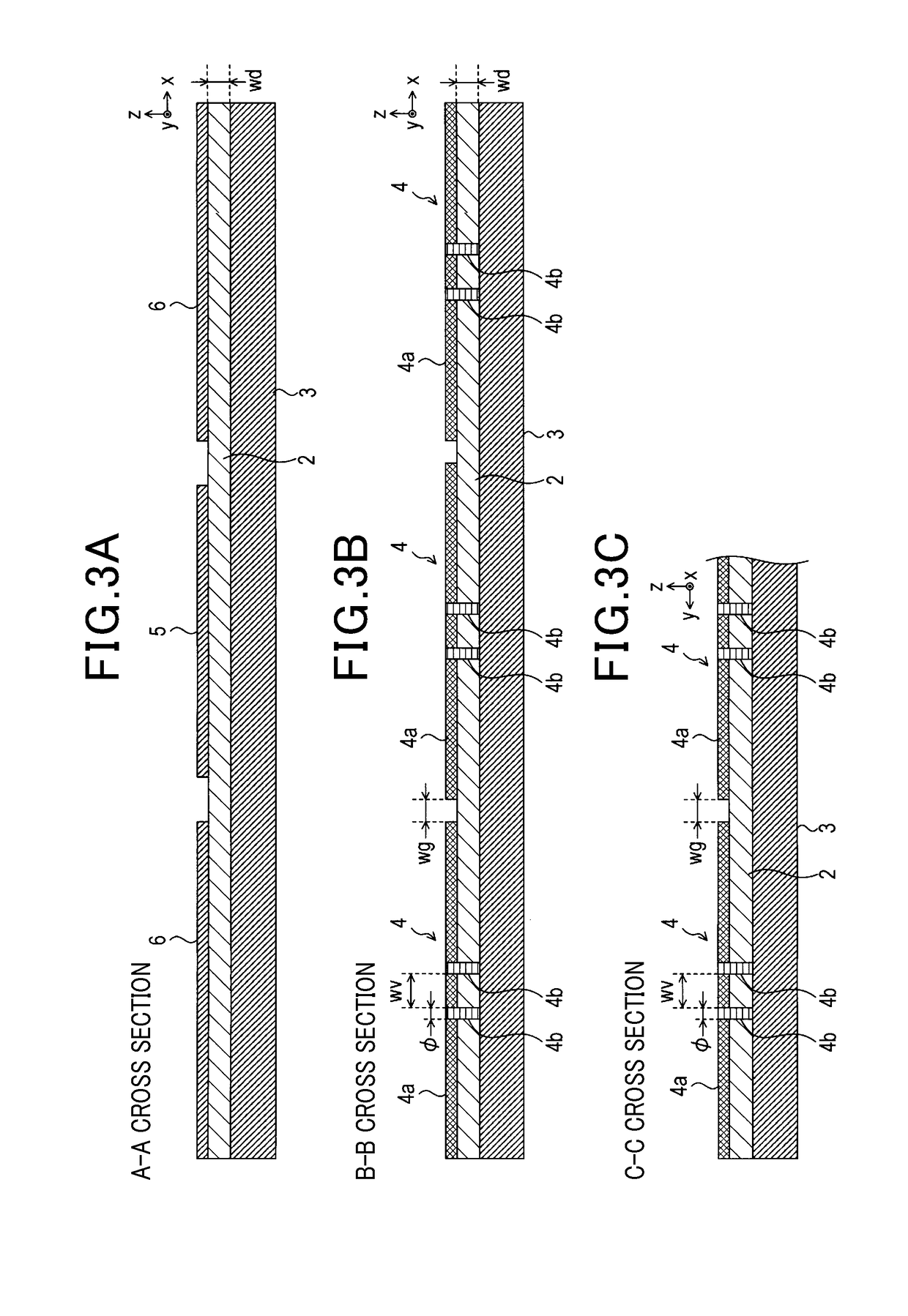
[0037]As illustrated in FIG. 1, in an antenna device 1 according to the present embodiment, a patch antenna 7, a conductor plate 6, and a plurality of EBGs 4 are formed on one face (a substrate front face) of a rectangular dielectric substrate 2. A ground plane 3 formed of a conductor is formed on the other face (a substrate rear face). As illustrated in FIG. 1, the present embodiment will be appropriately described using x-, y-, and z-axes of a three dimensional coordinate system, in which the origin point is the center part of the patch antenna 7 (the center part of a patch radiating element 5, described later), the x-axis is an axis passing the origin point and parallel with the short side of the dielectric substrate 2, the y-axis is an axis passing the origin point and parallel with the long side of the dielectric substrate 2, and the z-axis is an axis passing the origin point and perpendicular to the plate face of the dielectric substrate 2.

[0038]Note th...

second embodiment

[0087][Second Embodiment]

[0088]As illustrated in FIGS. 7A and 7B, in the present embodiment, two antenna devices 30 and 50 will be described. The two antenna devices 30 and 50 illustrated inFIGS. 7A and 7B have array structures of a plurality of conducting vias of an EBG different from that of the antenna device 1 according to the first embodiment illustrated in FIG. 1. The other configurations are the same as the configurations of the antenna device 1 according to the first embodiment.

[0089]First, the antenna device 30 illustrated in FIG. 7A will be described. In the antenna device 30 illustrated in FIG. 7A, a plurality of EBGs 31 each includes one patch-shaped pattern 31a and four conducting vias 31b. The shape and dimensions of the patch-shaped pattern 31a are the same as the shape and dimensions of the patch-shaped pattern 4a of the EBG 4 according to the first embodiment. The shape and dimensions of each of the four conducting vias 31b are the same as the shape and dimensions o...


PUM


Abstract

An antenna device includes: a dielectric substrate formed with a ground plane; a patch antenna having a dominant polarization direction in a predetermined direction on the dielectric substrate; at least one patch radiating element for supplying electric power provided on the patch antenna, the at least one patch radiating element being formed on the dielectric substrate; a patch-shaped conductor pattern formed on a substrate front face of the dielectric substrate on which the patch radiating element is formed; a plurality of connection conductors formed to penetrate the dielectric substrate for electrically connecting the conductor pattern to the ground plane; and a conductive structure having the conductor pattern and a plurality of the connection conductors. A plurality of the conductive structures is provided.

Description

CROSS-REFERENCE TO RELATED APPLICATION[0001]This application is based on and claims the benefit of priority from earlier Japanese Patent Application No. 2013-256083 filed Dec. 11, 2013, the description of which is incorporated herein by reference.BACKGROUND OF THE INVENTION[0002]Technical Field[0003]The present disclosure relates to an antenna device having a patch antenna.[0004]Background Art[0005]A patch antenna formed on a dielectric substrate has been used for a radar apparatus, for example, on a mobile unit, including a vehicle and an airplane, for monitoring the surroundings of the mobile unit. Commonly, in the configuration of a patch antenna, a patch radiating element (a patch-shaped conductor) is formed on a dielectric substrate. Generally, a conductor part serving as a ground plane is formed on a face of the dielectric substrate (in the following, referred to as “a substrate rear face”) on the opposite side of a face on which the patch radiating element is formed (in the f...

Claims


Application Information

Patent Timeline
Patent Type & Authority Patents(United States)
IPC IPC(8): H01Q9/04H01Q15/00H01Q1/48H01Q1/52
CPCH01Q9/0407H01Q15/008H01Q1/52H01Q1/48
Inventor KAWAGUCHI, KAZUSHIKONDO, ASAHI
Owner DENSO CORP
Features
  • R&D
  • Intellectual Property
  • Life Sciences
  • Materials
  • Tech Scout
  • Unparalleled Data Quality
  • Higher Quality Content
  • 60% Fewer Hallucinations
Learn More