Liquid crystal display device that avoids influence on image quality due to residual ions

a liquid crystal display and residual ions technology, applied in semiconductor devices, optics, instruments, etc., can solve the problems of deterioration of images, disappearance of persistence, and display device failure to display correct images, so as to prevent image persistence and high-quality image display

Active Publication Date: 2019-01-29
JAPAN DISPLAY INC
View PDF4 Cites 0 Cited by
  • Summary
  • Abstract
  • Description
  • Claims
  • Application Information

AI Technical Summary

Benefits of technology

[0007]The purpose of the present invention is to prevent the image persistence, thus realizes a liquid crystal display device having high quality image display.

Problems solved by technology

Sometimes a liquid crystal display device does not display correct images after the same image is displayed for a long time depending on certain images.
The image persistence disappears after certain time duration; however, it deteriorates the images until the image persistence disappears.

Method used


Image

  • Liquid crystal display device that avoids influence on image quality due to residual ions
  • Liquid crystal display device that avoids influence on image quality due to residual ions
  • Liquid crystal display device that avoids influence on image quality due to residual ions

Examples


first embodiment

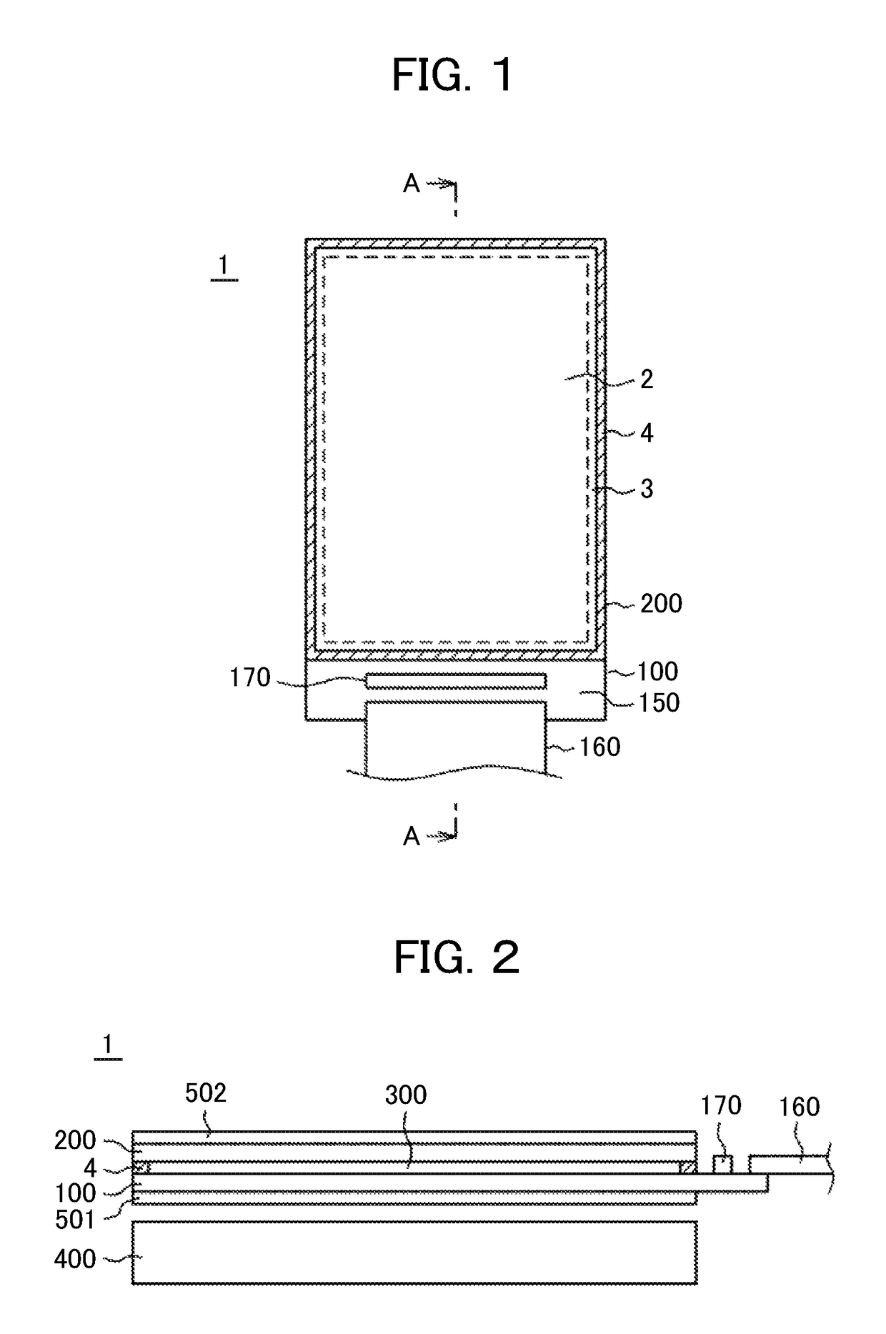
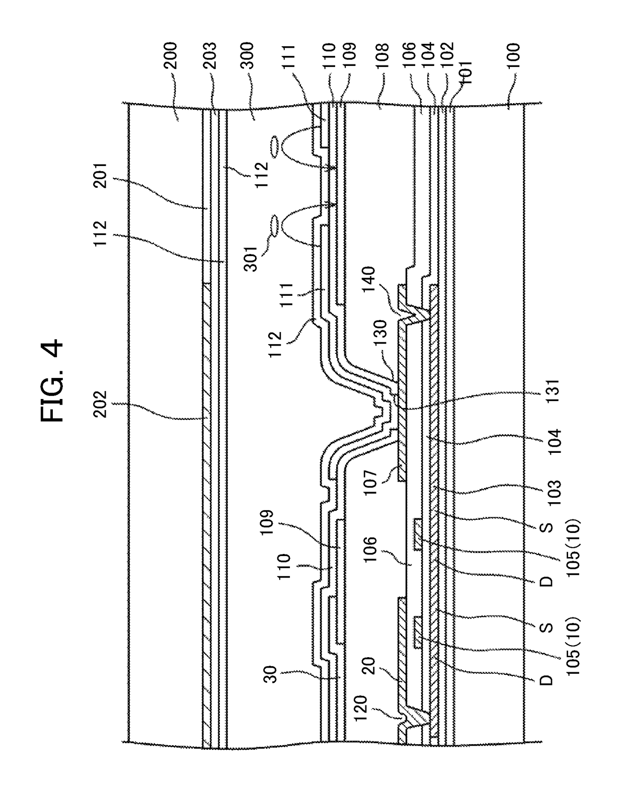
[0034]FIG. 1 is an example of a liquid crystal display device used e.g. in a cellar phone. FIG. 2 is a cross-sectional view along the line A-A of FIG. 1. In FIGS. 1 and 2, the TFT substrate 100 and the counter substrate 200 adhere to each other by the seal material 4; the liquid crystal 300 is sandwiched between the TFT substrate 100 and the counter substrate 200. The lower polarizing plate 501 is adhered to underneath the TFT substrate 100; the upper polarizing plate 502 is adhered to on the counter substrate 200. Since the liquid crystal is not self-illuminant, a back light is set on the back of the liquid crystal display panel.

[0035]The display area 2 is formed where the TFT substrate 100 and the counter substrate 200 overlap each other in a plan view; the area around the display area is the peripheral area 3. The seal material 4 is formed at the peripheral area to adhere the TFT substrate 100 and the counter substrate 200. The TFT substrate 100 is formed bigger than the counter ...

second embodiment

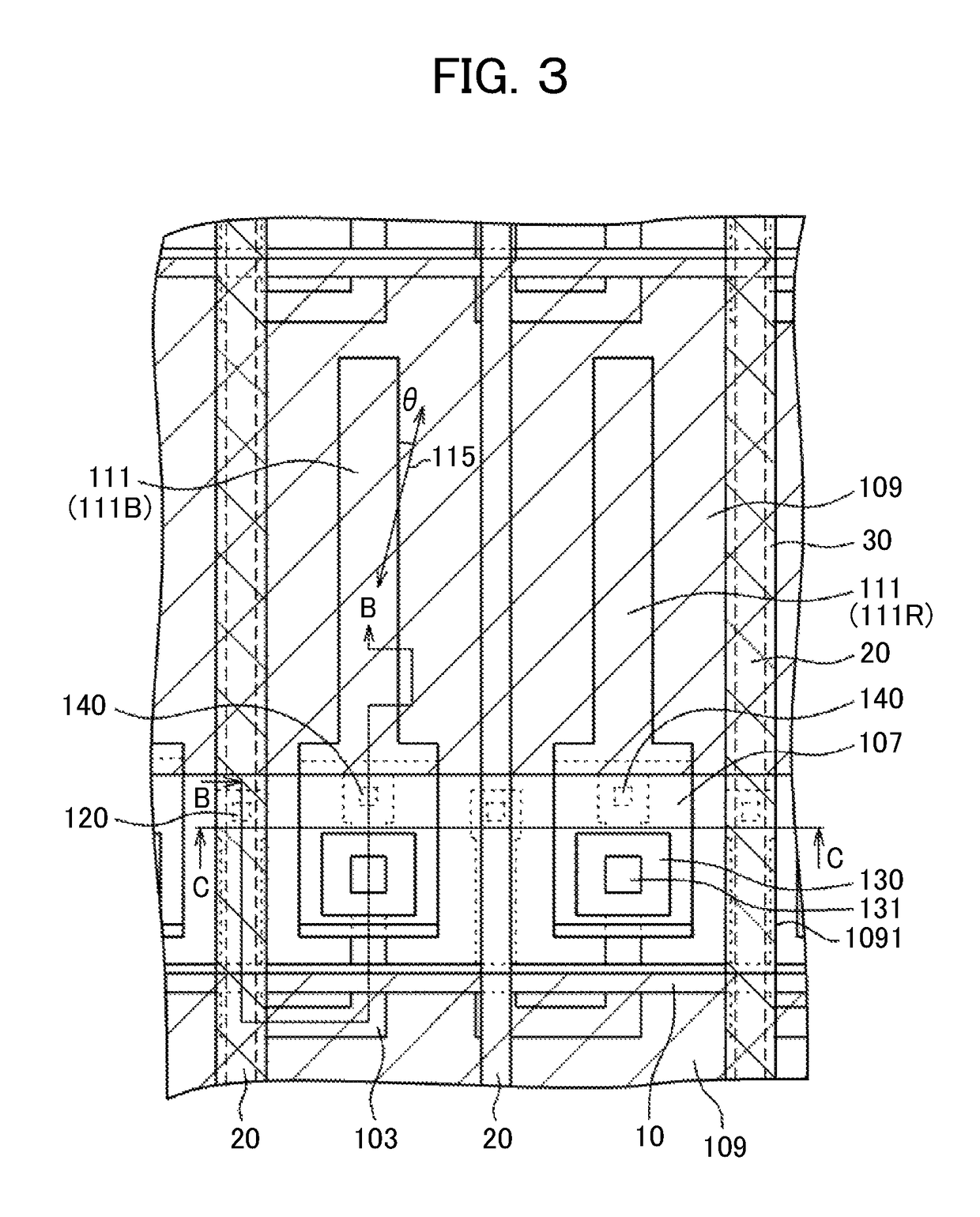
[0097]FIG. 17 is a plan view of the second embodiment. In FIG. 17, the scanning line 10 extends in lateral direction and the video signal lines 20 extend in longitudinal direction crossing the scanning line 10. The video signal lines are covered by the shield wirings. The insulating layer like the organic passivation layer is formed between the video signal lines and the shield wirings as explained in the first embodiment.

[0098]In FIG. 17, the shield wirings are formed by the first ITO 40, the second ITO 50 or the common metal wiring 30, etc. according to the positions. The shield wiring can be a laminated film as explained by FIGS. 12-16.

[0099]The pixel including the pixel electrode 111 is formed between the video signal line 20 and the adjacent video signal line 20. The first area of the pixel electrode 111 has two comb teeth with a slit between the comb teeth. The pixel electrode in FIG. 17 is an example; in other cases, the comb teeth can be one or three or more.

[0100]In FIGS. 1...


PUM

PropertyMeasurementUnit
distanceaaaaaaaaaa
distanceaaaaaaaaaa
distanceaaaaaaaaaa

Abstract

The purpose of the invention is to suppress image persistence. The structure if the invention is as follows: A liquid crystal display device comprising: scanning lines extending in a first direction and arranged in a second direction, video signal lines arranged to cross the scanning lines, a pixel area is surrounded by the scanning lines and the video signal lines, a pixel electrode is formed in the pixel area, wherein conductive wirings are formed over the video signal lines via an organic insulating film in a plan view in the display area where images are displayed, a width in the first direction of the conductive wiring is bigger than a width in the first direction of the video signal line, an amount that the conductive wiring protrude the video signal line in a plan view is essentially the same in both side of the video signal line.

Description

CLAIM OF PRIORITY[0001]The present application claims priority from Japanese Patent Application JP 2016-219682 filed on Nov. 10, 2016, the content of which is hereby incorporated by reference into this application.BACKGROUND OF THE INVENTION(1) Field of the Invention[0002]The present invention relates to a liquid crystal display device that measures image persistence due to ions.(2) Description of the Related Art[0003]A liquid crystal display device comprises a TFT substrate where thin film transistors (TFT) and pixel electrodes are formed and a counter substrate opposing to the TFT substrate, wherein a liquid crystal layer is sandwiched between the TFT substrate and the counter substrate. Images are formed by controlling the transmittance of light in each of pixels.[0004]Scanning lines extend in lateral direction and arranged in longitudinal direction, while image signal lines extend in longitudinal direction and arranged in lateral direction; wherein a pixel is formed in an area s...

Claims


Application Information

Patent Timeline
Patent Type & Authority Patents(United States)
IPC IPC(8): G02F1/1343H01L27/12G02F1/1368G02F1/1333G02F1/1362H01L29/786
CPCG02F1/134309G02F1/1368G02F1/133345G02F1/136227G02F1/136286H01L27/124G02F1/1362H01L29/78675G02F2001/13685G02F2001/133397G02F2001/134372G02F2001/136218G02F2001/136295G02F2201/122G02F2201/123G02F2202/104H01L29/78669G02F1/134372G02F1/136218G02F1/13685G02F1/133397G02F1/136295
Inventor MORIMOTO, MASATERUSAKAMOTO, MICHIAKISATO, TAKESHI
Owner JAPAN DISPLAY INC
Why Eureka
Try Eureka