Transistor, manufacturing method thereof, and display device including the same

a manufacturing method and transistor technology, applied in the direction of transistors, semiconductor devices, electrical devices, etc., can solve the problems of easy damage to the channel and caused by spatial limitation, and achieve the effect of reducing the space in which the transistor is located, reducing the size of the transistor, and facilitating the manufacture of high-resolution display devices

Active Publication Date: 2019-03-05
SAMSUNG DISPLAY CO LTD
View PDF9 Cites 0 Cited by
  • Summary
  • Abstract
  • Description
  • Claims
  • Application Information

AI Technical Summary

Benefits of technology

[0022]According to embodiments of the present disclosure, it is possible to minimize or reduce a size of a transistor irrespective of a length of a channel, thereby reducing a space in which the transistor is located. Accordingly, it is possible to easily manufacture a high-resolution display device.
[0023]In addition, it is possible to prevent characteristics of the transistor from deteriorating due to a hot carrier effect, or to reduce the likelihood thereof.
[0024]Further, it is possible to reduce a space for forming a capacitor. Accordingly, it is possible to easily manufacture a high-resolution display device.

Problems solved by technology

Because a channel formed in a semiconductor of the transistor is horizontally formed, and because the source electrode and the drain electrode are formed on the same layer, a spatial limitation is caused in forming them in the high-resolution display device.
In addition, because the channel of the transistor is horizontally formed, the channel may be easily damaged when a panel is bent.

Method used


Image

  • Transistor, manufacturing method thereof, and display device including the same
  • Transistor, manufacturing method thereof, and display device including the same
  • Transistor, manufacturing method thereof, and display device including the same

Examples


Embodiment Construction

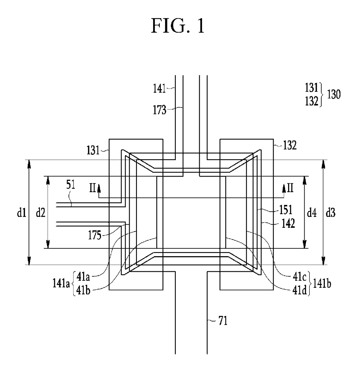
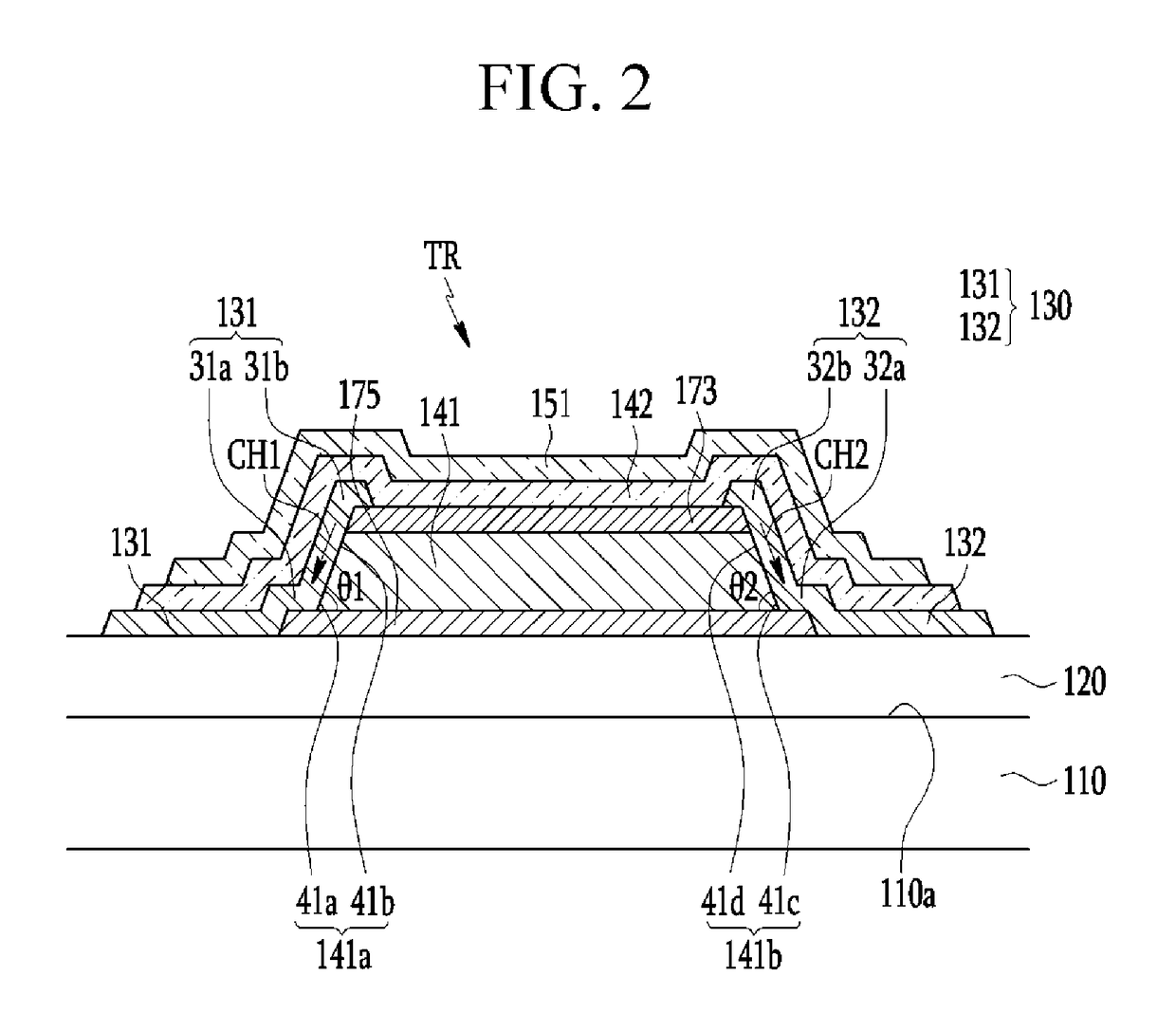
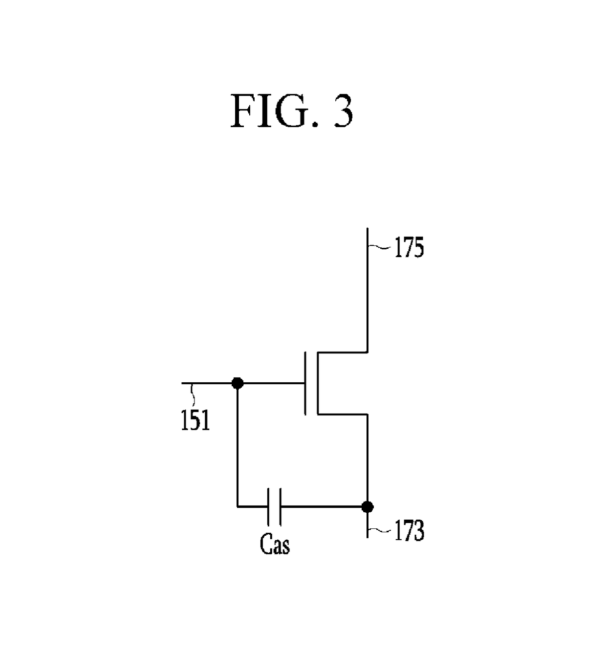
[0044]Embodiments of the present invention will be described more fully hereinafter with reference to the accompanying drawings, in which exemplary embodiments of the invention are shown. As those skilled in the art would realize, the described embodiments may be modified in various different ways, all without departing from the spirit or scope of the present invention.

[0045]To clearly describe the present invention, portions which do not relate to the description are omitted, and, unless otherwise noted, like reference numerals designate like elements throughout the specification.

[0046]The size and thickness of each component shown in the drawings may be arbitrarily shown for better understanding and ease of description, but the present disclosure is not limited thereto.

[0047]It will be understood that, although the terms “first,”“second,”“third,” etc., may be used herein to describe various elements, components, regions, layers, and / or sections, these elements, components, regions...


PUM


Abstract

An exemplary embodiment of the present disclosure provides a transistor including: a drain electrode; a first insulating member on the drain electrode and having a tilted side wall; a source electrode on the first insulating member; an active member covering the tilted side wall of the first insulating member, a side wall of the source electrode, and a side wall of the drain electrode; a second insulating member covering the source electrode and the active member; and a gate electrode on the second insulating member and overlapping the active member, wherein the active member defines a first channel region adjacent to the drain electrode and a second channel region adjacent to the source electrode, and wherein a width of the first channel region may be greater than that of the second channel region.

Description

CROSS-REFERENCE TO RELATED APPLICATION[0001]This application claims priority to and the benefit of Korean Patent Application No. 10-2016-0155240 filed in the Korean Intellectual Property Office on Nov. 21, 2016, the entire contents of which are incorporated herein by reference.BACKGROUND1. Field[0002]The present disclosure relates to a transistor, a manufacturing method thereof, and a display device including the same.2. Description of the Related Art[0003]Generally, a liquid crystal display (LCD), an organic light emitting diode (OLED) display, etc., are used as a display device.[0004]The display device includes a plurality of transistors and capacitors. Each transistor includes a gate electrode, a source electrode, a drain electrode, and a semiconductor.[0005]Because a channel formed in a semiconductor of the transistor is horizontally formed, and because the source electrode and the drain electrode are formed on the same layer, a spatial limitation is caused in forming them in th...

Claims


Application Information

Patent Timeline
Patent Type & Authority Patents(United States)
IPC IPC(8): H01L29/66H01L29/786H01L27/12H01L27/32
CPCH01L29/78696H01L27/1225H01L29/7869H01L29/78642H01L29/66969H01L27/3262H01L29/41733H01L29/42384H10K59/1213H01L27/1222H01L27/1237
Inventor KIM, JEE HOONYANG, SHIN HYUKLEE, KWANG SOO
Owner SAMSUNG DISPLAY CO LTD
Why Eureka
Try Eureka