Power semiconductor device

a technology of power semiconductors and power chips, applied in solid-state devices, printed circuit aspects, basic electric elements, etc., can solve the problems of related technique a and the extremely poor thermal dissipation properties of each power chip, and achieve the effect of suppressing thermal interference between power chips

Active Publication Date: 2019-03-12
MITSUBISHI ELECTRIC CORP
View PDF37 Cites 0 Cited by
  • Summary
  • Abstract
  • Description
  • Claims
  • Application Information

AI Technical Summary

Benefits of technology

[0009]It is an object of the present invention to provide a power semiconductor device capable of suppressing thermal interference between power chips.
[0011]According to the present invention, the IC is disposed at a center part of the package in a plan view, and the plurality of power chips are disposed so as to surround the IC in a plan view. In other words, the plurality of power chips are distributed around the IC. Thus, thermal interference between each power chip can be suppressed.

Problems solved by technology

Unfortunately, the related technique A has problems.
As a result, in the related technique A, each power chip has extremely poor thermal dissipation properties.

Method used


Image

  • Power semiconductor device
  • Power semiconductor device
  • Power semiconductor device

Examples


first preferred embodiment

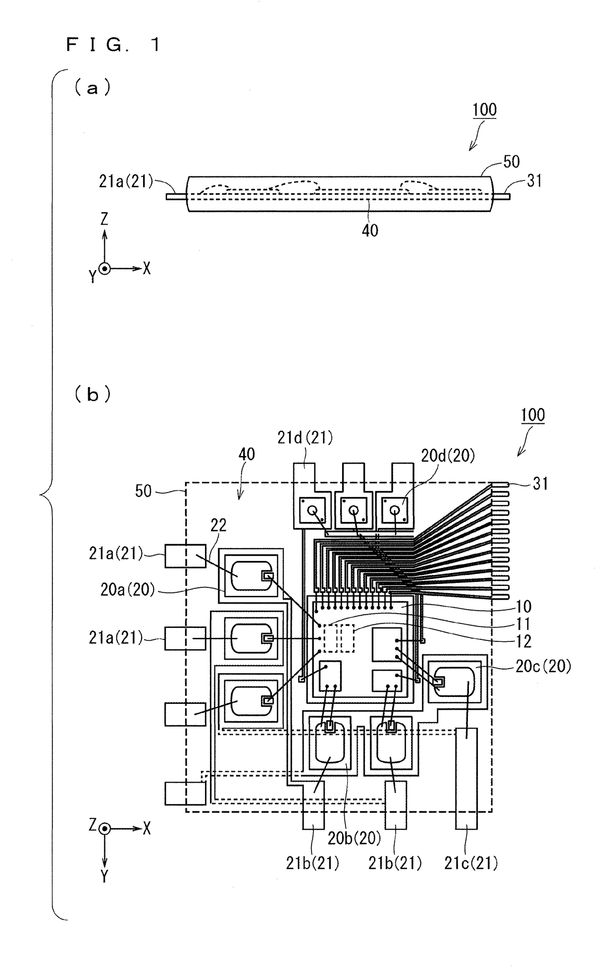
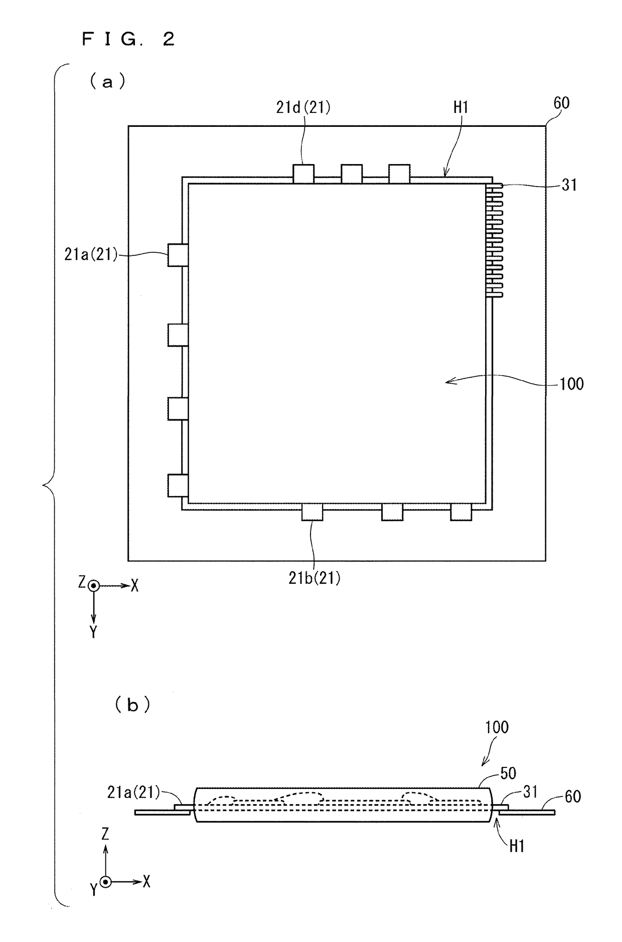
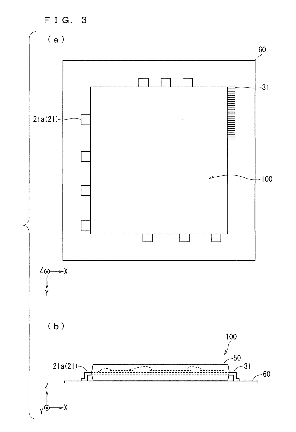
[0018]FIG. 1 is a diagram showing a power semiconductor device 100 according to a first preferred embodiment of the present invention. The power semiconductor device 100 is a power module that operates at a high voltage. A part (a) in FIG. 1 is a side view of the power semiconductor device 100. In the part (a) in FIG. 1, each of X, Y, and Z directions are orthogonal to one another. Moreover, in the drawings below, each of the X, Y, and Z directions are orthogonal to one another.

[0019]In the descriptions below, a direction including the X direction and an opposite direction thereof (−X direction) is also referred to as an X-axis direction. A direction including the Y direction and an opposite direction thereof (−Y direction) is also referred to as a Y-axis direction below. A direction including the Z direction and an opposite direction thereof (−Z direction) is also referred to as a Z-axis direction below.

[0020]A part (b) in FIG. 1 is a plan view showing an internal configuration of ...


PUM


Abstract

A power semiconductor device includes a plurality of power chips sealed in a package to control power and an IC sealed in the package to control each of the power chips. The IC is disposed at the center part of the package in the plan view. The plurality of power chips are disposed so as to surround the IC in the plan view.

Description

BACKGROUND OF THE INVENTION[0001]Field of the Invention[0002]The present invention relates to a power semiconductor device.[0003]Description of the Background Art[0004]A power semiconductor device functions as a power module supplying high power. The power semiconductor device is used for an inverter drive as one of main purposes. The power semiconductor device used for the inverter drive includes a plurality of power chips and an integrated circuit (IC) driving each of the power chips. The power chips are power semiconductor chips.[0005]Miniaturization of an area of a substrate in the power semiconductor device and cost reduction are required for the power semiconductor device.[0006]Japanese Patent Application Laid-Open No. 2012-074720 discloses a technique for reducing a size of the power semiconductor device (hereinafter, also referred to as a related technique A). Specifically, the related technique A discloses a technique for suitably packaging power chips and a control IC into...

Claims


Application Information

Patent Timeline
Patent Type & Authority Patents(United States)
IPC IPC(8): H01L23/495
CPCH01L23/49541H01L23/49562H01L23/49575H05K2201/10787H05K2201/10742H05K2201/1075H01L2924/13091H01L2924/13055H01L2224/48137H01L2224/48247H01L2924/1305H01L2924/00H01L2224/0603H01L23/28H01L23/31H01L25/18H01L27/07
Inventor NAKAGAWA, SHINYATANAKA, TOMOFUMI
Owner MITSUBISHI ELECTRIC CORP
Why Eureka
Try Eureka