Semiconductor module and inverter apparatus
A technology of semiconductors and inverters, which is applied in the field with a base plate, and can solve problems such as the temperature rise of the base plate 102, the cooling performance of the switching element 106 is reduced, and thermal interference is prone to occur.
- Summary
- Abstract
- Description
- Claims
- Application Information
AI Technical Summary
Problems solved by technology
Method used
Image
Examples
no. 1 approach
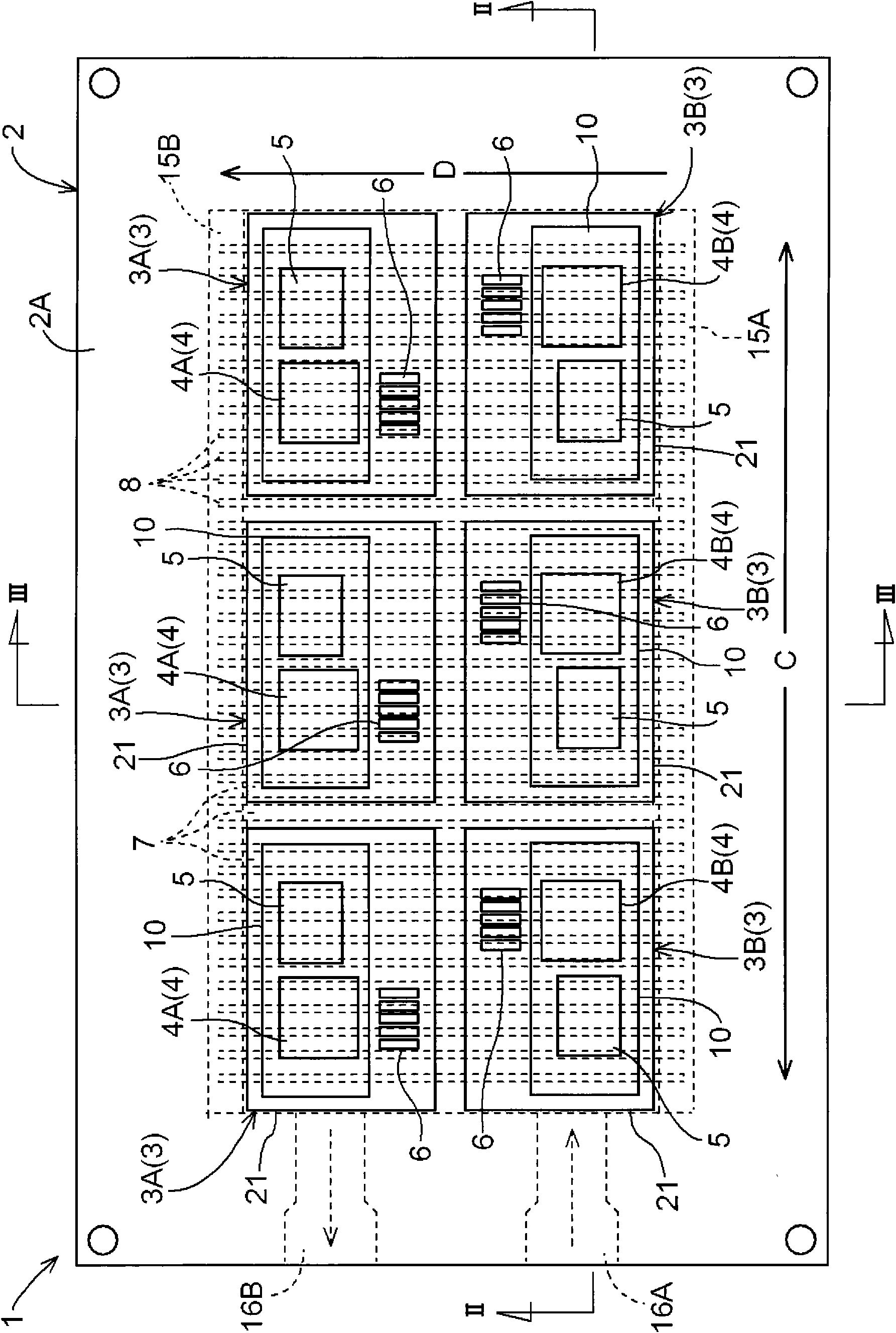
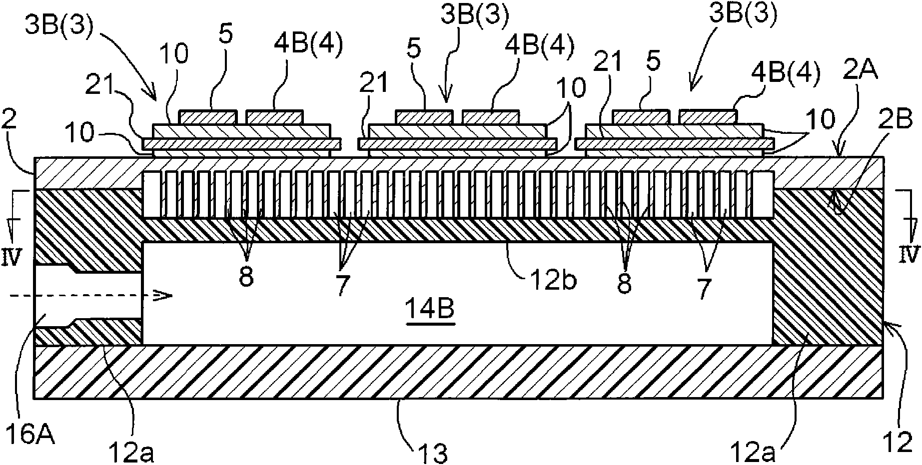
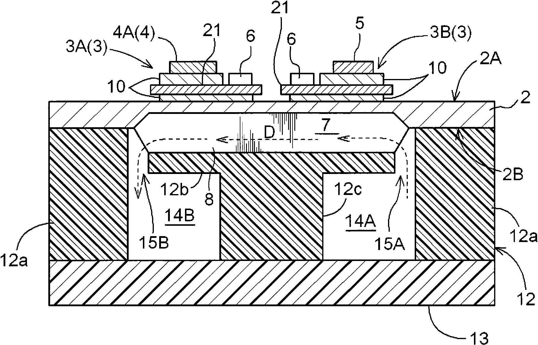
[0040] A first embodiment of the present invention will be described with reference to the drawings. In this embodiment, an example in which the present invention is applied to the semiconductor module 1 as an inverter device constituting a three-phase AC inverter circuit will be described. Figure 1 to Figure 8 It is a figure for demonstrating the structure of the semiconductor module 1 of this embodiment. Also, in Figure 1 to Figure 5 In , configurations other than the substrate 3 above the bottom plate 2 are omitted.
[0041] As shown in these figures, this semiconductor module 1 has a cooling structure including a coolant flow path 7 for cooling the switching element 4 of the substrate 3 placed on the upper surface 2A of the base plate 2, especially the most heat-generating. Allow to cool. Additionally, if Figure 6 As shown, this semiconductor module 1 constitutes an inverter circuit 11 for driving a three-phase AC motor 31 . Therefore, if figure 1 As shown, six s...
no. 2 approach
[0069] A second embodiment of the present invention will be described with reference to the drawings. Figure 9 It is a plan view showing the configuration of the main part of the semiconductor module 1 of the present embodiment. As shown in this figure, the semiconductor module 1 of this embodiment is configured such that only one set consisting of a pair of lower arm substrate 3A and upper arm substrate 3B is placed on one base plate 2 . That is, the semiconductor module 1 of this embodiment differs from the above-mentioned first embodiment in the number of substrates 3 mounted on one base plate 2 . In addition, the point which is not specifically demonstrated in this embodiment can be the same as the structure of the said 1st embodiment.
[0070] Therefore, in the semiconductor module 1 of this embodiment, compared with the semiconductor module 1 of the first embodiment, the width in the vertical direction C of the base plate 2 is narrowed, and the overall width W of the c...
no. 3 approach
[0072] A third embodiment of the present invention will be described with reference to the drawings. Figure 10 It is a plan view showing the configuration of the main part of the semiconductor module 1 of the present embodiment. The semiconductor module 1 of this embodiment is mainly different from the above-mentioned first and second embodiments in the configuration of the arrangement of the substrate 3 . Here, for the sake of simplification of drawings and the like, as in the above-mentioned second embodiment, only one set of a pair of substrates 3A, 3B is placed on one base plate 2 for description. In the same manner, it is also applicable to a configuration in which a pair of substrates 3A, 3B is used as a set and a plurality of sets of substrates 3 are placed on the bottom plate 2 . In addition, regarding the points not particularly described in this embodiment, the same configuration as that of the above-mentioned first embodiment or second embodiment can be employed. ...
PUM
 Abstract
Description
Claims
Application Information


