
Device structure for neuromorphic computing system

a computing system and neuromorphic technology, applied in computing models, biological models, instruments, etc., can solve the problem of large current consumption of total devices

Active Publication Date: 2019-03-26
MACRONIX INT CO LTD
View PDF40 Cites 30 Cited by
  • Summary
  • Abstract
  • Description
  • Claims
  • Application Information

AI Technical Summary

Benefits of technology

The patent describes a device called a neuromorphic memory that has resistance cells with transistors and resistive elements. The device also has peripheral circuits and sensing circuits to measure the resistance of the cells. The device has a layer of higher resistivity material in the contacts to reduce resistance. The transistors in the resistance cells can be either floating gate or dielectric charge trapping devices. The patent also describes methods for manufacturing the device. The technical effects of the invention include improved performance and reliability of the device, as well as reduced power consumption and improved efficiency.

Problems solved by technology

In the systems, there can be a very large number of inputs and outputs, so that the total current consumption can be very large.

Method used


Image

  • Device structure for neuromorphic computing system
  • Device structure for neuromorphic computing system
  • Device structure for neuromorphic computing system

Examples


first embodiment

[0050]FIG. 5A illustrates a row by four columns of resistance cells in an array of resistance cells having a number M of rows and a number N of columns of resistance cells on a substrate (e.g. 500) in accordance with a Each resistance cell in the row of resistance cells (e.g. 531A, 532A, 533A, 534A) has a transistor (e.g. 521) and a resistive element in series with the transistor. As shown in the example of FIG. 5A, a transistor (e.g. 521) in a resistance cell (e.g. 531A, 532A, 533A, 534A) is a floating gate device having a word line (e.g. WL1, WL2, WL3, WL4) and a floating gate (e.g. FG1, FG2, FG3, FG4), where the word line can act as a control gate over the floating gate. A transistor in a resistance cell can also be a dielectric trapping device, in an alternative embodiment. A first source line (e.g. SL1) is coupled to the transistors (e.g. 521 and 522) in resistance cells in two adjacent columns of resistance cells. A second source line (e.g. SL2) is coupled to the transistors ...

second embodiment

[0055]One difference is that in the second embodiment, the resistive elements (e.g. 581B, 582B, 583B, 584B) comprising the layer of higher resistivity material are disposed in a patterned resistive layer underlying and contacting the bit lines (e.g. BL1) and overlying and contacting upper ends of the interlayer conductors (e.g. 571, 572, 573, 574). In patterned resistive layer, the resistive elements (e.g. 581B, 582B, 583B, 584B) are physically separated from each other.

[0056]FIG. 5C illustrates a row by four columns of resistance cells in an array of resistance cells having a number M of rows and a number N of columns of resistance cells in accordance with a third embodiment. Each resistance cell in the row of resistance cells (e.g. 531C, 532C, 533C, 534C) has a transistor and a resistive element in series with the transistor. Description about like elements in the first embodiment, including the substrate, the transistors in the resistance cells, the source lines and the bit lines...

third embodiment

[0057]One difference is that in the third embodiment, the resistive elements (e.g. 581C, 582C, 583C, 584C) comprising the layer of higher resistivity material are disposed beneath and contacting lower ends of the interlayer conductors (e.g. 571-574) in a substrate. The device comprises peripheral circuits such as sense amplifiers (e.g. 780, FIG. 7) that can have contacts in a substrate. Contacts of the peripheral circuits in a substrate have a lower resistance than the resistive elements comprising the layer of higher resistivity material in the resistance cells in the array of resistance cells.

[0058]FIG. 5D illustrates a row by four columns of resistance cells in an array of resistance cells having a number M of rows and a number N of columns of resistance cells in accordance with a fourth embodiment. Each resistance cell in the row of resistance cells (e.g. 531D, 532D, 533D, 534D) has a transistor and a resistive element in series with the transistor. Description about like elemen...


PUM


Abstract

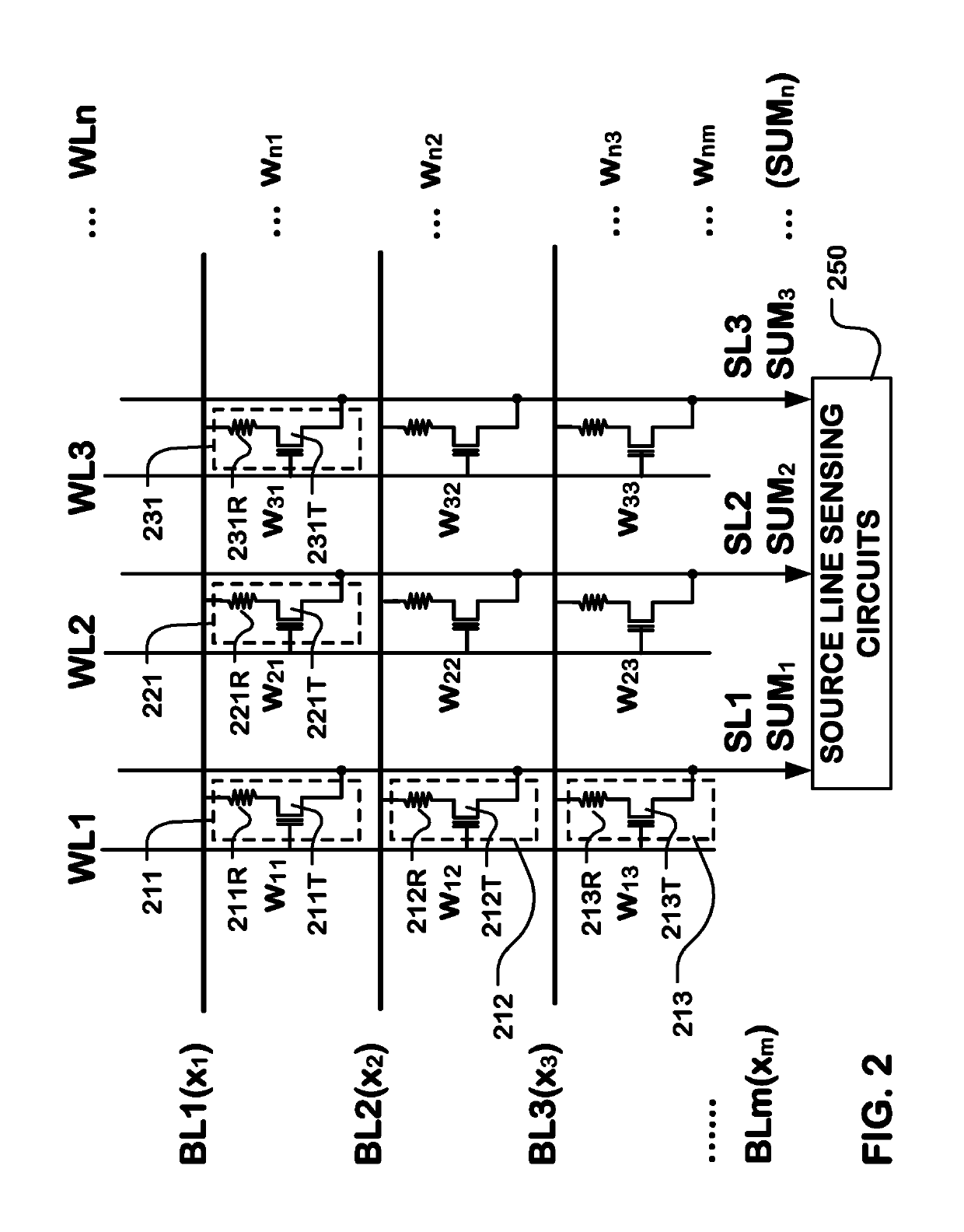
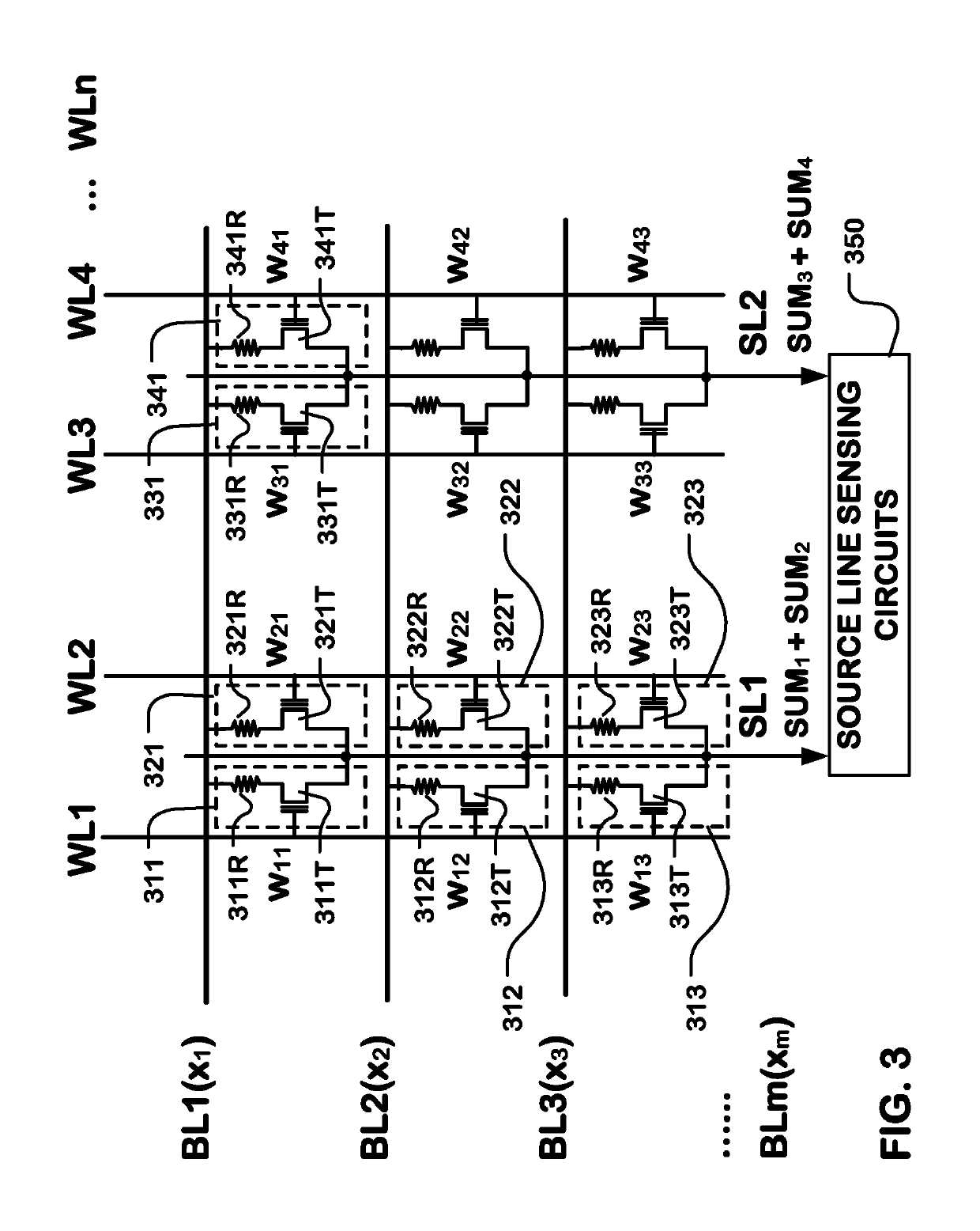
An array of resistance cells has a number M of rows and a number N of columns of resistance cells. Each cell comprises a transistor having a threshold, representing a weight factor Wnm of the cell, and a resistive element in series with the transistor. Each cell has a cell resistance having a first value when the transistor is on and a second value when the transistor is off. A set of source lines is coupled to the resistance cells in respective columns. A set of bit lines is coupled to the resistance cells in respective rows, signals on the bit lines representing inputs x(m) to the respective rows. A set of word lines is coupled to gates of the transistors in the resistance cells in respective columns. Current sensed at a particular source line represents a sum of products of the inputs x(m) by respective weight factors Wnm.

Description

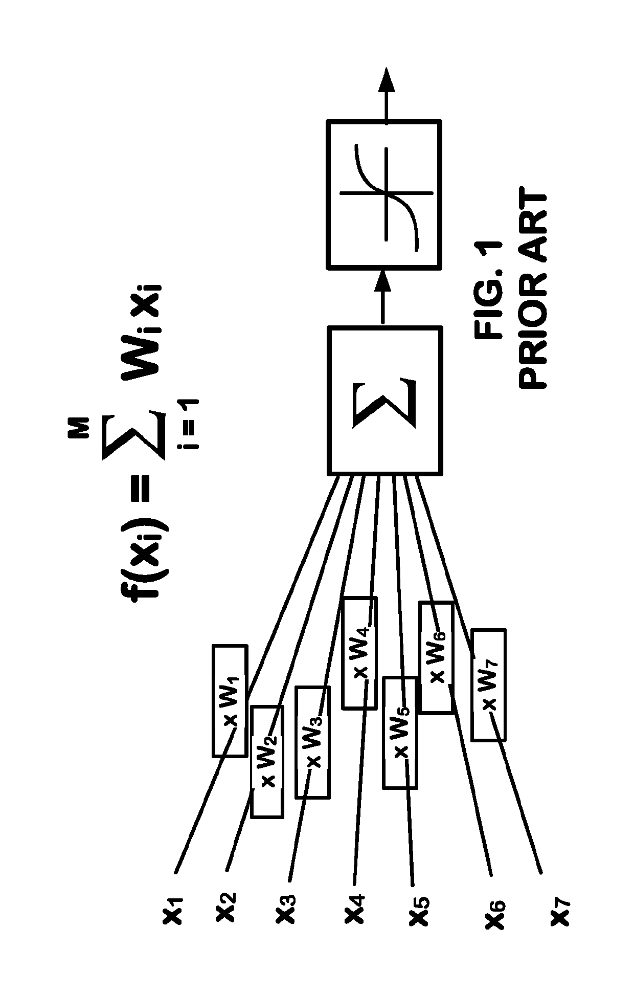
BACKGROUNDField[0001]The present invention relates to circuitry that can be used to perform sum-of-products operations.Description of Related Art[0002]In neuromorphic computing systems, machine learning systems and circuitry used for some types of computation based on linear algebra, the sum-of-products function can be an important component. The function can be expressed as follows:[0003]f⁡(xi)=∑i=1M⁢Wi⁢xi[0004]In this expression, each product term is a product of a variable input Xi and a weight Wi. The weight Wi can vary among the terms, corresponding for example to coefficients of the variable inputs Xi.[0005]The sum-of-products function can be realized as a circuit operation using cross-point array architectures in which the electrical characteristics of cells of the array effectuate the function.[0006]For high-speed implementations, it is desirable to have a very large array so that many operations can be executed in parallel, or very large sum-of-products series can be perfor...

Claims


Application Information

Patent Timeline
IPC IPC(8): G11C13/00H01L27/24G06N3/063H01L45/00
CPCG11C13/004H01L27/2436H01L27/2463G06N3/063H01L45/16G11C13/0069G11C2213/79G06N3/065H10B63/30H10B63/80H10N70/011
Inventor LIN, YU-YULEE, FENG-MIN
Owner MACRONIX INT CO LTD
Learn More