

Semiconductor device and method of manufacturing the same
a technology of semiconductor devices and semiconductor bodies, applied in the direction of acceleration measurement using interia forces, acceleration measurement in multiple dimensions, instruments, etc., can solve the problem of change in capacitance between the detection frame and the detection electrode, suppress the application of stress, and suppress the displacement of movable structural bodies in the in-plane direction
- Summary
- Abstract
- Description
- Claims
- Application Information
AI Technical Summary
Benefits of technology
Problems solved by technology
Method used
Image

Examples
first embodiment
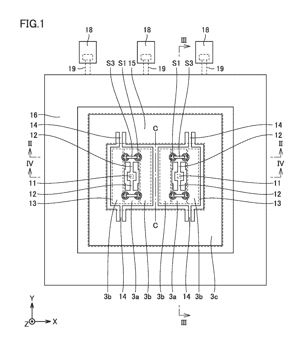
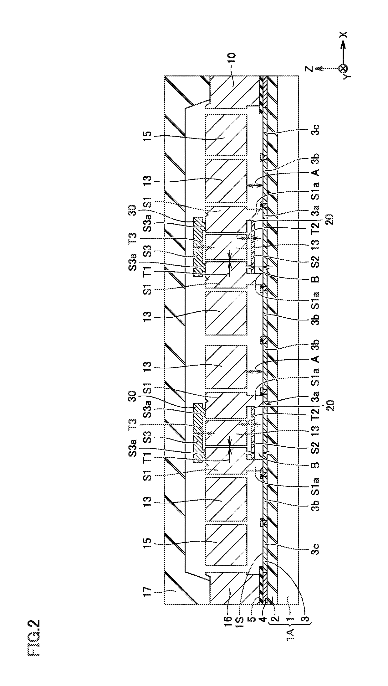
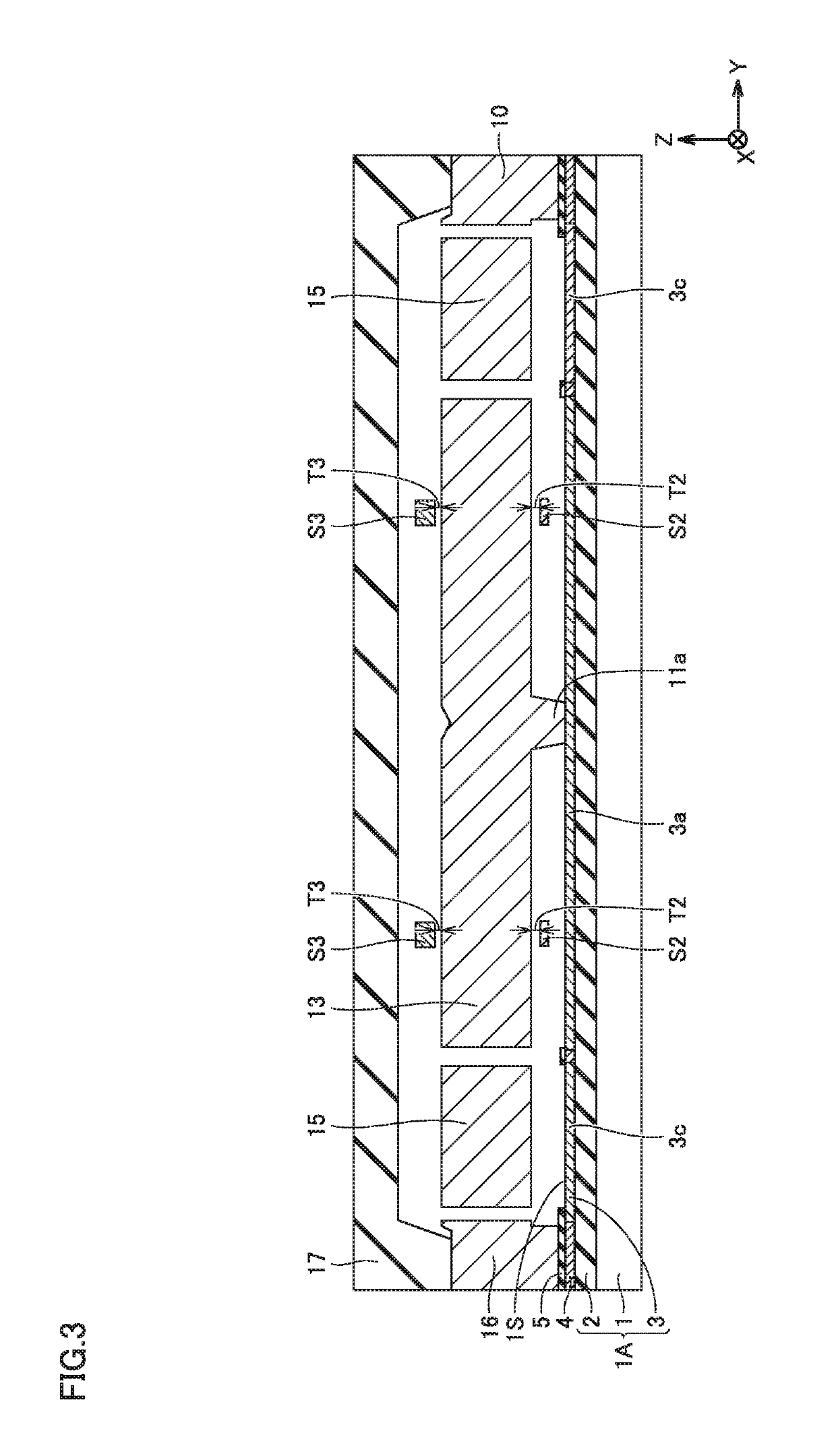
[0045]First, the configuration of an acceleration sensor as a semiconductor device of the present embodiment is described using FIGS. 1 to 4. It is noted that an X direction, a Y direction and a Z direction are introduced for convenience of explanation. In FIG. 1, the X direction is a direction in which two movable structural bodies 13 are adjacent to each other. In the X direction, the rightward direction in FIG. 1 is the positive direction (+X direction), and the leftward direction in FIG. 1 is the negative direction (−X direction). The Y direction is a direction orthogonal to the X direction, and is a direction in which a beam 12 and a link beam 14 extend. In the Y direction, the upward direction in FIG. 1 is the positive direction (+Y direction), and the downward direction in FIG. 1 is the negative direction (−Y direction). The Z direction is a direction orthogonal to both the X direction and the Y direction, and is an up-and-down direction orthogonal to a surface 1S of a substr...
second embodiment
[0089]Next, an acceleration sensor as a semiconductor device of a second embodiment of the present invention is described. In the following, the configuration and the manufacturing method of the present embodiment are substantially the same as the configuration and the manufacturing method of the first embodiment unless otherwise described, and therefore, the same elements are designated by the same reference characters and description thereof will not be repeated.
[0090]With reference to FIGS. 18 and 19, the acceleration sensor of the present embodiment is mainly different in the arrangement of first stopper member S1, second stopper member S2 and third stopper member S3, as compared to the acceleration sensor of the first embodiment shown in FIGS. 1 and 2. It is noted that cap 17 is not shown in FIG. 18 for clarity.
[0091]In the acceleration sensor of the first embodiment, first stopper members S1 are arranged at positions shifted from beam 12 in the Y direction. In contrast, in the...
third embodiment
[0095]Next, an acceleration sensor as a semiconductor device of a third embodiment of the present invention is described. In the following, the configuration and the manufacturing method of the present embodiment are substantially the same as the configuration and the manufacturing method of the first embodiment unless otherwise described, and therefore, the same elements are designated by the same reference characters and description thereof will not be repeated.
[0096]With reference to FIGS. 20 and 21, in the first embodiment, first stopper member S1 formed of conductive film 30 and third stopper member S3 formed of conductive film 30 constitute a stacked structure. It is noted that cap 17 is not shown in FIG. 20 for clarity. In contrast, in the present embodiment, first stopper member S1 and third stopper member S3 are formed of the same film. First stopper member S1 and third stopper member S3 are formed to enclose movable structural body 13. It is noted that, with reference to F...
PUM
| Property | Measurement | Unit |
|---|---|---|
| distance | aaaaa | aaaaa |
| thickness | aaaaa | aaaaa |
| acceleration | aaaaa | aaaaa |
Abstract
Description
Claims
Application Information