OLED touch-control substrate and fabrication method thereof, and display apparatus

a technology of touch control substrate and fabrication method, which is applied in the field of display technologies, can solve the problems of large module thickness, high production cost, and low light transparency, and achieve the effect of relatively low production cost and relatively large light transmittan

Active Publication Date: 2019-04-16
BOE TECH GRP CO LTD +1
View PDF12 Cites 0 Cited by
  • Summary
  • Abstract
  • Description
  • Claims
  • Application Information

AI Technical Summary

Benefits of technology

[0008]The first touch-control electrodes and the second touch-control electrodes configured for realizing a touch-control function are embedded in the OLED touch-control substrate. Thus, the thickness of the modules of the OLED touch-control substrate may be significantly reduced; the light transmittance may be increased; and the production cost may be reduced.
[0020]The thicknesses of the modules of the OLED touch-control substrate fabricated by the disclosed method may be relatively small; and the light transmittance may be relatively large. Further, comparing with existing methods, the production cost may be relatively low.

Problems solved by technology

Such a technology has many disadvantages, such as large module thickness, low light transparency and high production cost, etc.

Method used


Image

  • OLED touch-control substrate and fabrication method thereof, and display apparatus
  • OLED touch-control substrate and fabrication method thereof, and display apparatus
  • OLED touch-control substrate and fabrication method thereof, and display apparatus

Examples


Embodiment Construction

[0036]For those skilled in the art to better understand the technical solution of the invention, reference will now be made in detail to exemplary embodiments of the invention, which are illustrated in the accompanying drawings. Wherever possible, the same reference numbers will be used throughout the drawings to refer to the same or like parts.

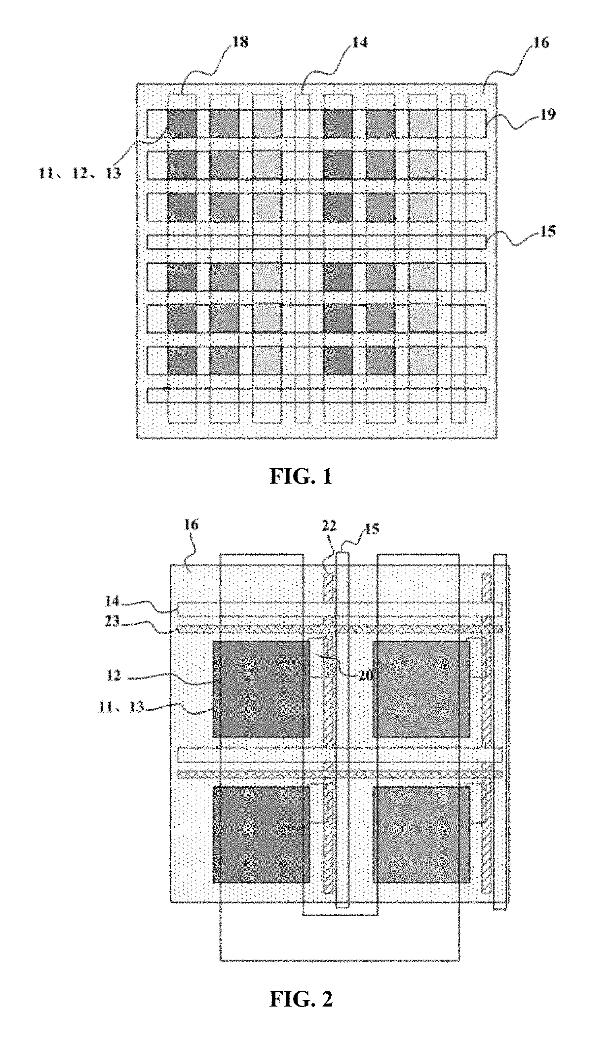
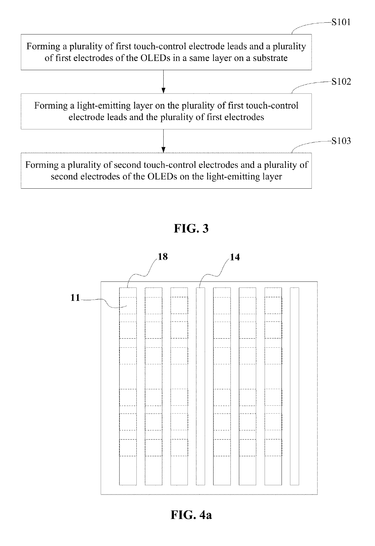
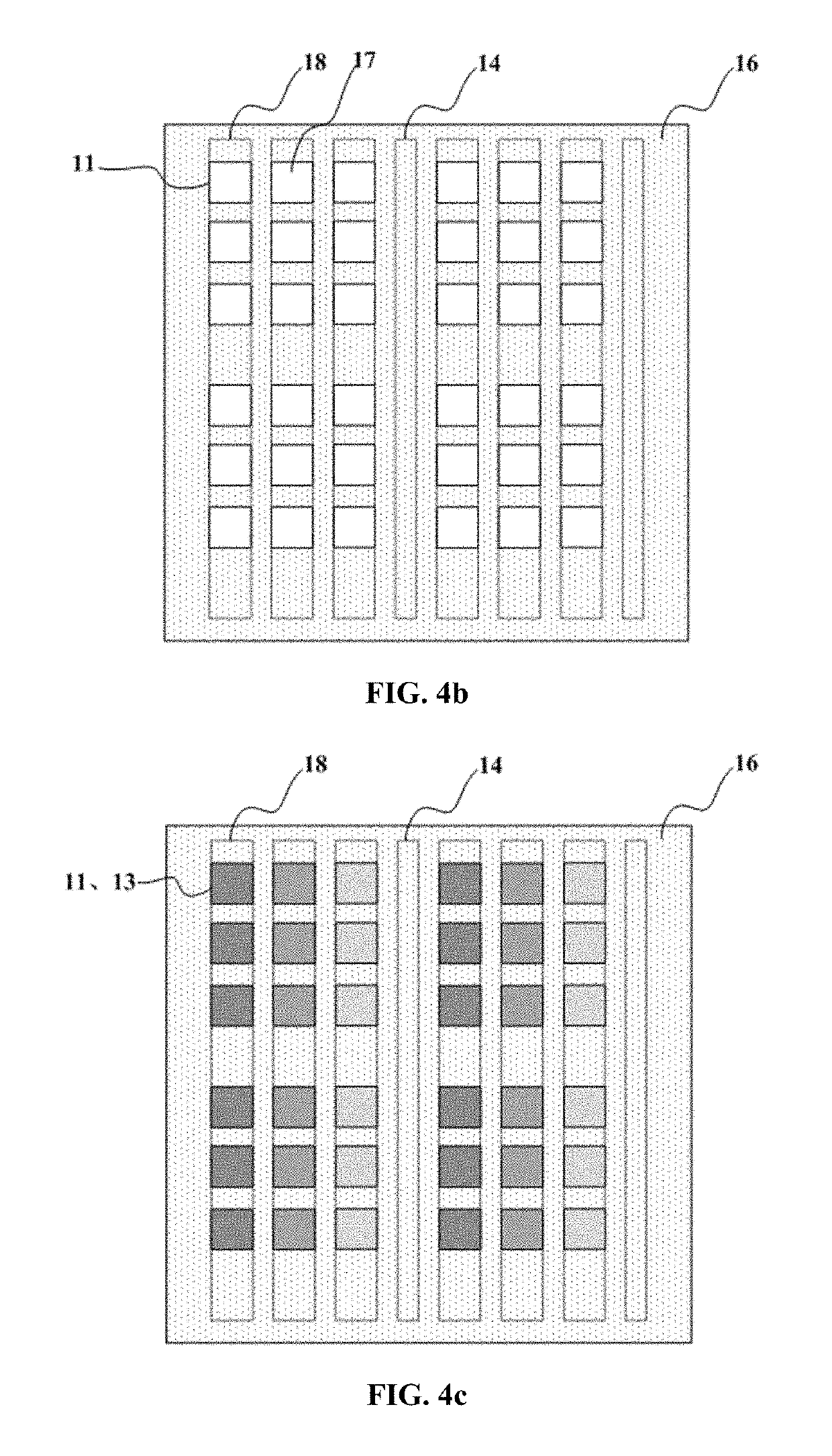
[0037]In order to reduce the thicknesses of the modules of OLED touch-control substrate, and to increase the light transmittance and lower the production cost, an OLED touch-control substrate and a fabrication process thereof are provided in the present disclosure.

[0038]According to driving methods, OLEDs can be categorized as Passive Matrix OLEDs (PMOLEDs) and Active Matrix OLED (AMOLEDs). For PMOLEDs, the anodes and cathodes form a matrix, and pixels in the matrix are turned on / off by a scanning mode. Each pixel is operated under a short pulse mode; and the emission of light in the PMOLEDs is a transient process with a relatively high light...


PUM


Abstract

An organic light-emitting diode (OLED) touch-control substrate is provided. The organic light-emitting diode (OLED) touch-control substrate comprises a plurality of OLEDs, each of the OLEDs having a first electrode, a second electrode and a light-emitting layer between the first electrode and the second electrode; a plurality of first touch-control electrodes disposed in a same layer with the first electrodes and insulated from the first electrode lines; and a plurality of second touch-control electrodes disposed in a same layer with the second electrodes and insulated from the second electrode lines and the first touch-control electrodes.

Description

CROSS-REFERENCES TO RELATED APPLICATIONS[0001]This application is a national phase entry under 35 U.S.C. § 371 of International Application No. PCT / CN2015 / 097029, filed on Dec. 10, 2015, which claims priority to Chinese Patent Application No. 201510144816.6, filed on Mar. 30, 2015. The above enumerated patent applications are incorporated by reference herein in their entirety.FIELD OF THE INVENTION[0002]The present invention generally relates to the field of the display technologies and, more particularly, to an OLED touch-control substrate and fabrication methods thereof, and a display apparatus.BACKGROUND[0003]Organic Light-Emitting Diode (OLED) displays have many advantages, including ultra-thin, light weight, low cost, wide viewing-angle, self-emitting, continuously adjustable emitting color, fast response speed, low driving voltage, low power-consumption, broad working temperature range, simple manufacturing process, high light-emitting efficiency, and flexible display, etc. Th...

Claims


Application Information

Patent Timeline
Patent Type & Authority Patents(United States)
IPC IPC(8): G06F3/041H01L51/56H01L27/32G06F3/044
CPCH01L27/323G06F3/044G06F3/0412H01L27/3288H01L51/56H01L27/3276G06F2203/04103G06F3/0445G06F3/0446H10K59/40H10K59/131H10K59/179H10K71/00
Inventor DONG, XIANGDANHUANG, WEIYUN
Owner BOE TECH GRP CO LTD
Why Eureka
Try Eureka