Image sensor, manufacturing method of image sensor, camera module and manufacturing method of camera module

An image sensor and pixel layer technology, applied in the field of structured light, can solve the problems of increasing camera modules, affecting production efficiency, and numerous camera module installation procedures, reducing module thickness, improving production efficiency, and ensuring color imaging quality. Effect

Inactive Publication Date: 2019-06-14
TRULY OPTO ELECTRONICS
View PDF7 Cites 0 Cited by
  • Summary
  • Abstract
  • Description
  • Claims
  • Application Information

AI Technical Summary

Problems solved by technology

However, on the one hand, the camera filter increases the thickness of the camera module, and on the other hand, since the filter needs to be arranged between the lens group and the image sensor, the installation process of the camera module is complicated, which affects the production efficiency.

Method used


Image

  • Image sensor, manufacturing method of image sensor, camera module and manufacturing method of camera module
  • Image sensor, manufacturing method of image sensor, camera module and manufacturing method of camera module
  • Image sensor, manufacturing method of image sensor, camera module and manufacturing method of camera module

Examples


Embodiment 1

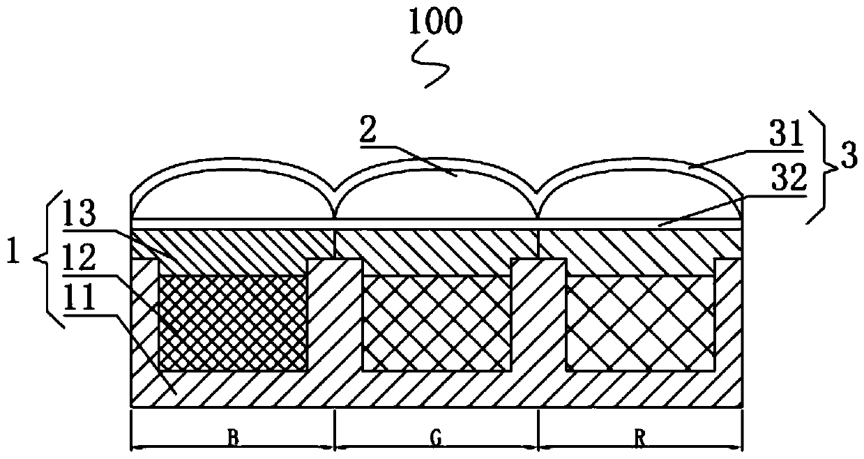
[0031] Such as figure 1 As shown, it represents an image sensor 100 provided by the present invention. The image sensor 100 includes a pixel layer 1 and a microlens layer 2 disposed on the pixel layer 1 ; a filter film 3 is provided on the surface of the microlens layer 2 .

[0032] In this way, since the filter film 3 is directly arranged on the microlens layer 2 of the image sensor 100, such an image sensor 100 can directly realize the filtering function through the filter film 3 when receiving light, so that it can be used in camera modules. In the group, the setting of the optical filter can be omitted, which effectively reduces the thickness of the module, reduces the installation process, and improves production efficiency.

[0033] More specifically, in this embodiment, the filter film 3 includes an infrared filter film 31 and an antireflection film 32 . More specifically, the infrared filter film 31 is arranged on the side of the microlens layer 2 facing the pixel la...

Embodiment 2

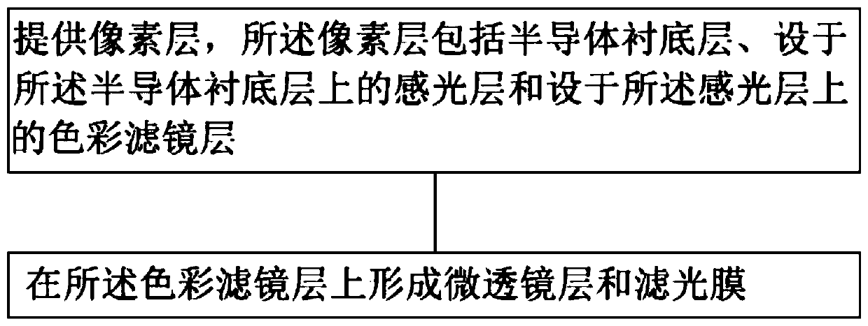
[0036] Such as figure 2 As shown, it shows a manufacturing method of an image sensor provided in this embodiment. The preparation method comprises the following steps:

[0037] Step 1: providing a pixel layer, the pixel layer including a semiconductor substrate layer, a photosensitive layer disposed on the semiconductor substrate layer, and a color filter layer disposed on the photosensitive layer;

[0038] Step 2: forming a microlens layer and a filter film on the color filter layer.

[0039] More specifically, the filter film includes an infrared filter film and an anti-reflection film, and the step 2 includes: step 2.1: forming an anti-reflection film on the color filter layer; step 2.2, forming an anti-reflection film on the anti-reflection film A microlens layer is formed on the microlens layer; specifically, the material of the microlens layer can be organic material or glass; step 2.3: forming an infrared filter film on the microlens layer.

[0040] In this way, by ...

Embodiment 3

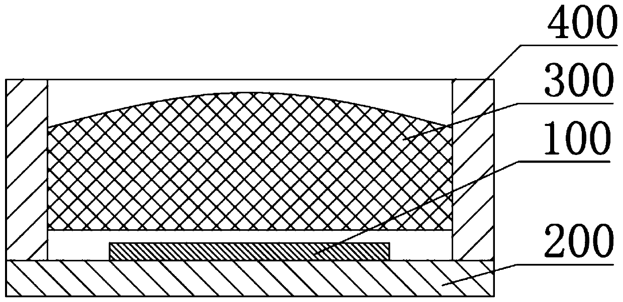
[0042] Such as image 3 As shown, it shows a camera module provided by this embodiment, which includes the image sensor 100 described in the above embodiment, and also includes a circuit board 200 electrically connected to the image sensor 100, and is arranged on the image sensor The lens group 300 on the incident light line 100 and the carrier 400 supporting the lens group 300 .

[0043] In this way, since in this embodiment, the microlens layer of the image sensor 100 is provided with a filter film, so that such an image sensor 100 can directly achieve the filtering effect through the filter film when receiving light. The camera module provided eliminates the need for filter settings, which calmly and effectively reduces the thickness of the camera module, reduces the installation process, and improves production efficiency.

[0044] Moreover, since the arrangement of the optical filter is omitted, the arrangement of the base for supporting the optical filter can also be re...


PUM


Abstract

The invention provides an image sensor. The image sensor comprises a pixel layer and a micro-lens layer, wherein a light filter film is arranged on the surface of the micro-lens layer. The invention further provides a manufacturing method of the image sensor. The manufacturing method of the image sensor comprises the steps of 1, providing the pixel layer, wherein the pixel layer comprises a semiconductor substrate layer, a photosensitive layer arranged on the semiconductor substrate layer and a color filter layer arranged on the photosensitive layer; and 2, forming the micro-lens layer and thelight filter film on the color filter layer. The invention further provides a camera module. The camera module comprises the image sensor, a circuit board, a lens group and a carrier. The invention further provides a manufacturing method of the camera module. The manufacturing method of the camera module comprises the steps of providing the circuit board and the image sensor; fixing the image sensor to the circuit board; providing the lens group and the carrier; screwing the lens group into the carrier; and fixing the carrier fixedly provided with the lens group to the circuit board providedwith the image sensor. A light filter can be removed, so that the thickness of the module is reduced, and the production efficiency is improved.

Description

technical field [0001] The invention relates to the technical field of structured light, in particular to an image sensor, a camera module and a manufacturing method thereof. Background technique [0002] With the rapid development of recognition technologies such as face recognition, the application range of camera modules is becoming wider and wider. In the camera module, the photoelectric conversion is generally realized by the image sensor, and in order to have a better imaging effect, the existing camera module is often provided with a filter between the lens group and the image sensor. Setting the filter can realize the filtering of light and better meet the imaging needs. However, on the one hand, the imaging filter increases the thickness of the camera module, and on the other hand, because the filter needs to be arranged between the lens group and the image sensor, the installation process of the camera module is complicated, which affects the production efficiency...

Claims


Application Information

Patent Timeline
IPC IPC(8): H01L27/146H04N5/225
Inventor 郑礼旺
Owner TRULY OPTO ELECTRONICS
Why Eureka
Try Eureka