Member for optical scanner, optical scanner, method of manufacturing optical scanner, image display device, and head-mounted display

a technology of optical scanners and parts, applied in the direction of optics, optical elements, instruments, etc., can solve the problems of adversely affecting the wiring line, and achieve the effect of reducing the drive voltage, increasing the swing angle of the movable portion 21, and reducing the driving for

Active Publication Date: 2019-06-25
SEIKO EPSON CORP
View PDF11 Cites 19 Cited by
  • Summary
  • Abstract
  • Description
  • Claims
  • Application Information

AI Technical Summary

Benefits of technology

[0081]The wiring line connected to the piezoresistive element may be provided instead of the wiring line 42. That is, although the wiring line 42 forming the coil 32 is thinner than the structure 61 in the embodiment, an embodiment of the invention is not limited to this. The invention may employ a form in which the wiring line connected to the piezoresistive element is provided instead of the wiring line 42 forming the coil 32 and the wiring line connected to the piezoresistive element is thinner than the structure 61. Such a form also provides the advantageous effects described above. In this case, a magnet, instead of the coil 32, is bonded to the second movable portion 212, and thus a driving force for driving the movable portion 21 can be obtained.
[0082]The two permanent magnets 31 and 31 placed on the base (not shown) are provided outside the support portion 22. The permanent magnets 31 become magnetized in oblique directions with respect to the oscillation axis J1 and the oscillation axis J2 in the plan view. The permanent magnets 31 are disposed such that the N-pole of one of the permanent magnets 31 and the S-pole of the other permanent magnet 31 are opposite to each other. The permanent magnets 31 and the coil 32 described above constitute a drive unit that drives the movable portion 21.
[0083]That is, the drive unit includes the permanent magnets 31 and the coil 32, and rotatably drives the movable portion 21 described above by an electromagnetic drive method (more specifically, a moving coil-type electromagnetic drive method). The electromagnetic drive method can generate a large driving force. Therefore, the drive unit employing the electromagnetic drive method can increase the swing angle of the movable portion 21 while lowering a drive voltage.
[0084]The permanent magnet 31 is not particularly limited, and for example, a magnetized hard magnetic substance, such as a neodymium magnet, a ferrite magnet, a samarium-cobalt magnet, an alnico magnet, or a bonded magnet, can be favorably used.
[0085]The coil 32 is electrically connected to a power supply (not shown). To the coil 32, a superimposed voltage including a first alternating voltage and a second alternating voltage superimposed on each other is applied. The first alternating voltage causes the first movable portion 211 to oscillate about the oscillation axis J1, and the second alternating voltage causes the second movable portion 212 together with the first movable portion 211 to oscillate about the oscillation axis J2. With this configuration, the first movable portion 211 oscillates about the oscillation axis J1 while the second movable portion 212 oscillates about the oscillation axis J2; as a result, the first movable portion 211 oscillates about the oscillation axes J1 and J2. It is preferable that the oscillation of the first movable portion 211 about the oscillation axis J1 is resonantly driven, and that the oscillation of the second movable portion 212 about the oscillation axis J2 is non-resonantly driven. As the waveform of the first alternating voltage, a sine wave of approximately 10 kHz or more and 40 kHz or less is preferably used. As the waveform of the second alternating voltage, a sawtooth wave of approximately 30 Hz or more and 120 Hz or less (approximately 60 Hz) is preferably used. With this configuration, the oscillation of the light reflective portion 213 is a movement suitable for drawing an image.2. Method of Manufacturing Optical Scanner
[0086]Hereinafter, a method of manufacturing an optical scanner will be described using, by way of example, the manufacture of the optical scanner 1 described above.

Problems solved by technology

However, when the mask is disposed on the first surface, the mask may come in contact with the wiring line and adversely affect the wiring line.

Method used


Image

  • Member for optical scanner, optical scanner, method of manufacturing optical scanner, image display device, and head-mounted display
  • Member for optical scanner, optical scanner, method of manufacturing optical scanner, image display device, and head-mounted display
  • Member for optical scanner, optical scanner, method of manufacturing optical scanner, image display device, and head-mounted display

Examples


first modified example

of Member for Optical Scanner

[0123]The structure preventing the contact between the mask and the wiring line may be provided in a position different from that of FIG. 1.

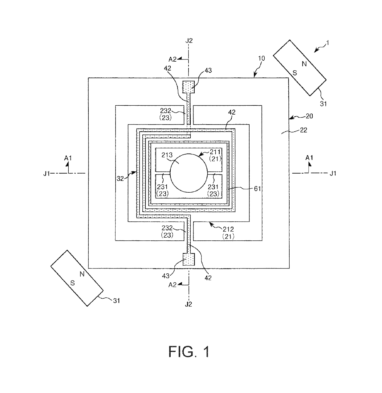
[0124]FIG. 10 is a plan view showing a first modified example of the optical scanner 1 and the member 10 for an optical scanner shown in FIG. 1. FIG. 11 is a cross-sectional view taken along the line B-B in FIG. 10. In the following description, differences from the optical scanner 1 and the member 10 for an optical scanner shown in FIGS. 1 and 2 are mainly described, and a description of similar configurations is omitted. Moreover, in FIGS. 10 and 11, the configurations similar to those of FIGS. 1 and 2 are denoted by the same reference numerals and signs.

[0125]The member 10 for an optical scanner shown in FIG. 10 includes, when the wiring line 42 is defined as a first wiring line, a second wiring line 42A that is different from the wiring line 42. In the member 10 for an optical scanner shown in FIG. 10, the second...

second modified example

of Member for Optical Scanner

[0135]FIG. 12 is a plan view showing a second modified example of the optical scanner 1 and the member 10 for an optical scanner shown in FIG. 1. FIG. 13 is a cross-sectional view taken along the line C-C in FIG. 12. In the following description, differences from the optical scanner 1 and the member 10 for an optical scanner shown in FIGS. 1 and 2 are mainly described, and a description of similar configurations is omitted. Moreover, in FIGS. 12 and 13, the configurations similar to those of FIGS. 1 and 2 are denoted by the same reference numerals and signs.

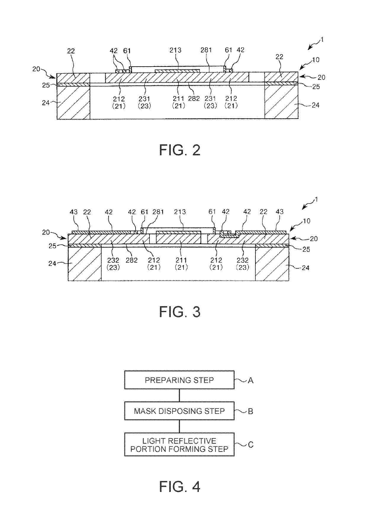
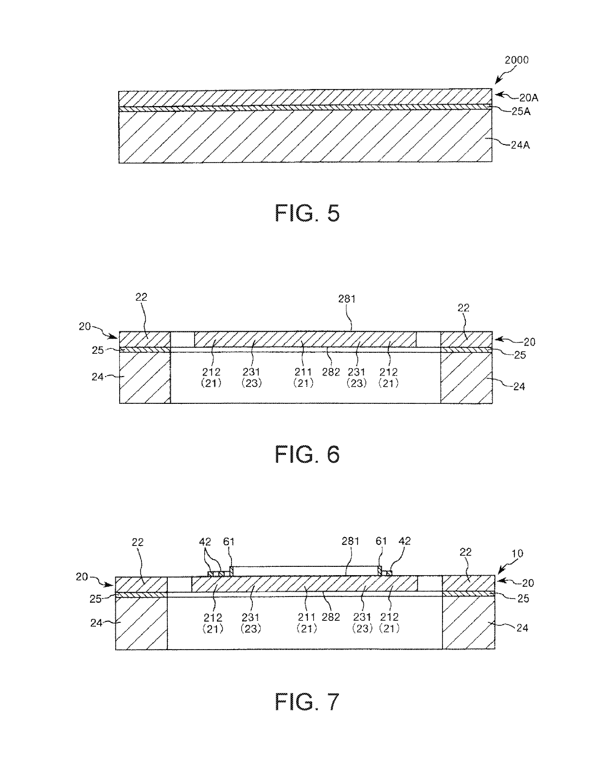
[0136]The member 10 for an optical scanner shown in FIG. 13 includes six structures 61 provided on the first major surface 281 of the support portion 22. The member 10 for an optical scanner including the structures 61 can prevent the contact between the mask and the wiring line 42 in forming the light reflective portion 213 on the first major surface 281 of the first movable portion 211 by various ki...

application example 1

of Image Display Device

[0156]FIG. 15 is a perspective view showing Application Example 1 of the image display device.

[0157]As shown in FIG. 15, the image display device 9 can be applied to a portable image display device 100.

[0158]The portable image display device 100 includes a casing 110 formed with dimensions allowing a user to hold the casing with hand, and the image display device 9 incorporated in the casing 110. The portable image display device 100 can display a predetermined image on a predetermined surface of, for example, a screen, a desk, or the like.

[0159]The portable image display device 100 includes a display 120 that displays predetermined information, a keypad 130, an audio port 140, control buttons 150, a card slot 160, and an AV port 170.

[0160]The portable image display device 100 may have other functions such as a communication function and a GPS reception function.


PUM


Abstract

A member for an optical scanner includes: a functional portion including a movable portion, a shaft portion oscillatably supporting the movable portion, and a support portion supporting the shaft portion; a wiring line provided on the movable portion; and a structure provided on the functional portion and thicker than the wiring line; the wiring line and the structure are provided on a first major surface of the functional portion.

Description

BACKGROUND[0001]1. Technical Field[0002]The present invention relates to a member for an optical scanner, an optical scanner, a method of manufacturing an optical scanner, an image display device, and a head-mounted display.[0003]2. Related Art[0004]As one of optical scanning means used in projectors or head-mounted displays, an optical scanners is known (e.g., see JP-A-2008-170565).[0005]An oscillator device disclosed in JP-A-2008-170565 includes a movable plate, a beam, and a support substrate. The support substrate supports the movable plate through the beam, and the movable plate freely vibrates. On a first surface of the movable plate, a light reflective surface for reflecting light is provided. The light reflected on the light reflective surface can be deflected by two-dimensionally vibrating the movable plate with the oscillator device.[0006]Moreover, a sensor that measures a desired detection physical quantity is disposed in a portion on the first surface of the movable plat...

Claims


Application Information

Patent Timeline
Patent Type & Authority Patents(United States)
IPC IPC(8): G02B26/10G02B26/08G02B27/01
CPCG02B26/101G02B26/085G02B27/0101G02B27/0172G02B26/105G02B2027/0178
Inventor HINO, MAKIKOMIZOGUCHI, YASUSHI
Owner SEIKO EPSON CORP
Why Eureka
Try Eureka