Array substrate preparation method, array substrate, and organic light-emitting display device

A technology for light-emitting display devices and array substrates, which is applied in the manufacture of semiconductor devices, electric solid-state devices, semiconductor/solid-state devices, etc., can solve problems such as complex processes, and achieve the effects of simplifying the manufacturing process, reducing pixel size, and saving costs

Active Publication Date: 2015-06-17
CHENGDU VISTAR OPTEOLECTRONICS CO LTD
View PDF9 Cites 31 Cited by
  • Summary
  • Abstract
  • Description
  • Claims
  • Application Information

AI Technical Summary

Problems solved by technology

[0006] In the prior art, the formation of each layer of thin film transistors and capacitors needs to undergo an etching process covered by multiple masks, and the process is complicated.

Method used


Image

  • Array substrate preparation method, array substrate, and organic light-emitting display device
  • Array substrate preparation method, array substrate, and organic light-emitting display device
  • Array substrate preparation method, array substrate, and organic light-emitting display device

Examples


Embodiment Construction

[0072] The present invention will be further described below in conjunction with the accompanying drawings and specific embodiments, so that those skilled in the art can better understand the present invention and implement it, but the examples given are not intended to limit the present invention.

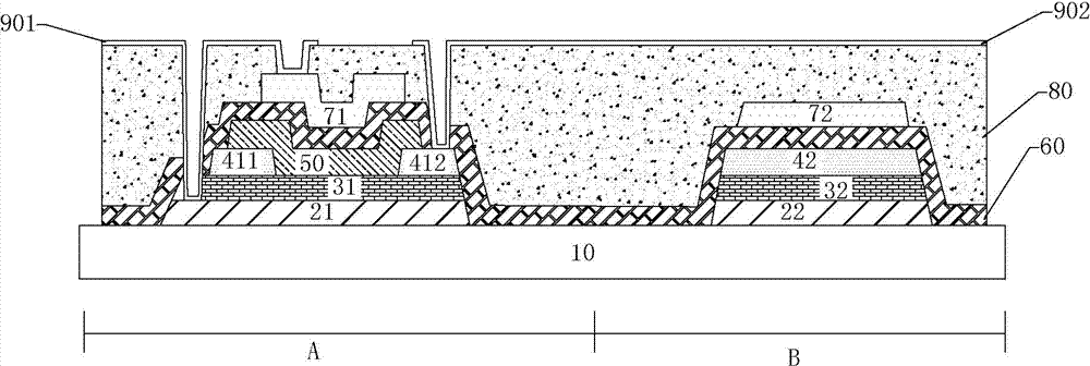
[0073] Since the formation process of the array substrate in the prior art needs to go through multiple masks and etching processes, the manufacturing process is complicated. electrode, source electrode and drain electrode, and simultaneously form the first electrode and the second electrode of the capacitor, and multiple masking and etching steps can be omitted. And using the preparation method, the present invention provides an array substrate with a double-gate thin film transistor, and the array substrate also has a capacitor with two capacitors connected in parallel, so as to increase the driving force and increase the capacitance.

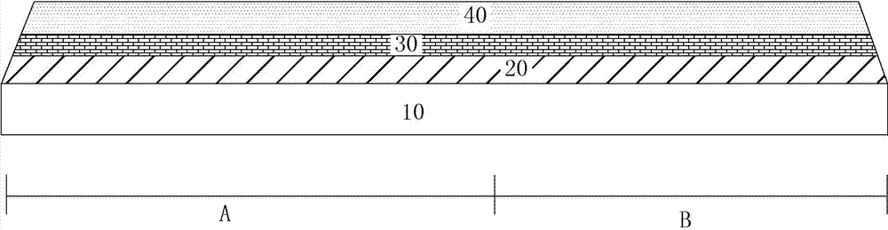
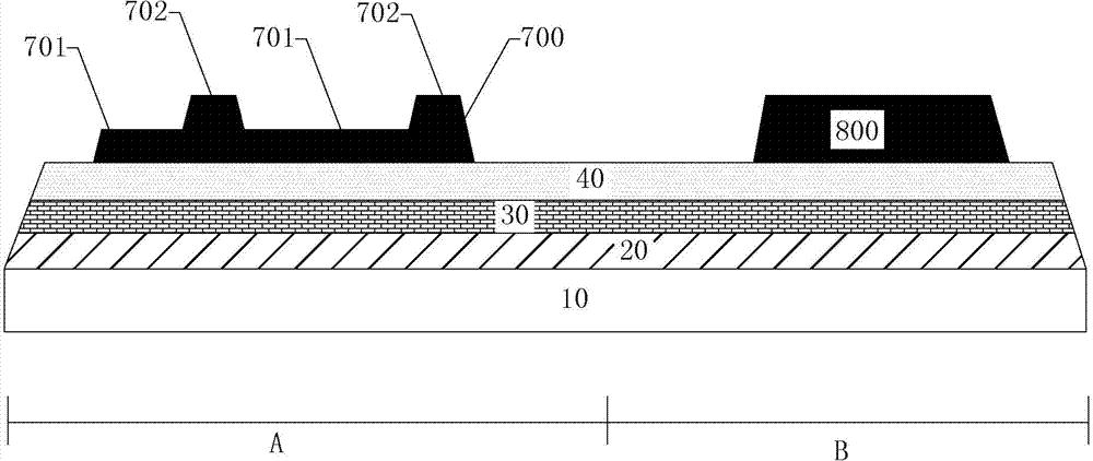
[0074] combine Figure 1~11 As shown, as ...


PUM


Abstract

The invention discloses an array substrate preparation method, an array substrate, and an organic light-emitting display device. The preparation method comprises the following steps: (1) sequentially forming a first metal layer, a first insulating material layer and a second metal layer, which cover a thin-film transistor region and a capacitor device region, on a substrate; and (2) etching the second metal layer, the first insulating material layer and the first metal layer with photoresist and a half-tone mask on the second metal layer, forming a source and a drain which are separated, a gate insulating layer and a bottom gate in the thin-film transistor region, and forming a second electrode, a first dielectric layer and a first electrode in the capacitor device region. Thus, the source, the drain, the gate insulating layer and the bottom gate of the thin-film transistor can be etched by one half-tone mask, the second electrode, the first dielectric layer and the first electrode of the capacitor device are formed at the same time, and the process is simplified. The array substrate of the invention has a dual-gate thin-film transistor and a capacitor device connected in parallel with two capacitors. The capacitor capacity is improved on the basis of increasing the driving force.

Description

technical field [0001] The invention belongs to the field of organic light-emitting display devices, and in particular relates to a method for preparing an array substrate, an array substrate prepared by the method, and an organic light-emitting display device composed of the array substrate. Background technique [0002] An organic light emitting display device (OLED) displays images by using organic light emitting elements. When the excitons generated by the combination of electrons and holes in the organic emission layer drop from the excited state to the ground state, a certain amount of energy is released to generate light, and an organic light-emitting display device (OLED) displays images by using this light. [0003] Generally speaking, an organic light-emitting display device (OLED) needs to use a plurality of thin film transistors, at least one of which requires high current driving characteristics to ensure a stable supply of current required for light emission of...

Claims


Application Information

Patent Timeline
Patent Type & Authority Applications(China)
IPC IPC(8): H01L21/77H01L27/12H01L27/32
CPCH01L27/1214H01L27/13H01L21/77H10K59/12
Inventor 蔡伟民陆海峰
Owner CHENGDU VISTAR OPTEOLECTRONICS CO LTD
Why Eureka
Try Eureka