Method for controlling resistivity and N-type silicon single crystal

a technology of resistivity and silicon single crystal, which is applied in the direction of crystal growth process, polycrystalline material growth, chemistry apparatus and processes, etc., can solve the problems of high cost of epw, difficult to uniformly distribute fz method in axial direction, and difficulty in increasing crystal diameter, etc., to inhibit the reduction of yield and high precision

Active Publication Date: 2019-09-03
SHIN-ETSU HANDOTAI CO LTD
View PDF22 Cites 1 Cited by
  • Summary
  • Abstract
  • Description
  • Claims
  • Application Information

AI Technical Summary

Benefits of technology

[0022]As mentioned above, the present invention can inhibit the reduction in yield even if dislocation occurs during silicon single crystal growth and can control the resistivity of a silicon single crystal with high precision.

Problems solved by technology

Unfortunately, EPW is expensive since an additional step (an epitaxial growth step) is included compared with CZ-PW (a wafer produced by the CZ method), and the FZ method has a difficulty in increasing a crystal diameter.
However, a silicon single crystal produced by the CZ method causes a segregation phenomenon, so that it is difficult to uniform its resistivity distribution in an axial direction (a pulling axial direction).
However, boron (B) has a segregation coefficient of about 0.78, which is larger than the segregation coefficient of phosphorus (P), and thus cannot be used in the above techniques.

Method used


Image

  • Method for controlling resistivity and N-type silicon single crystal
  • Method for controlling resistivity and N-type silicon single crystal
  • Method for controlling resistivity and N-type silicon single crystal

Examples


example 1

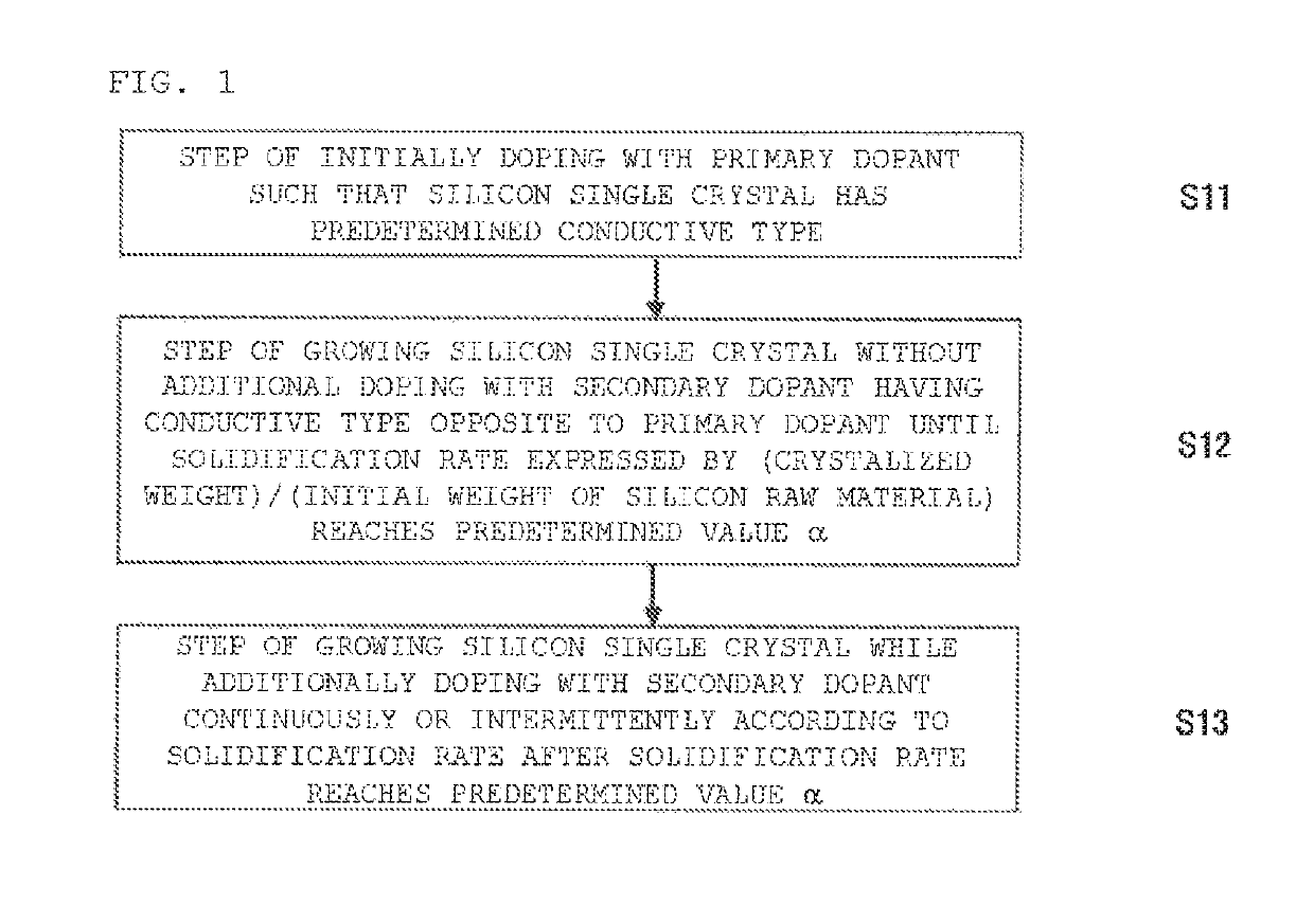
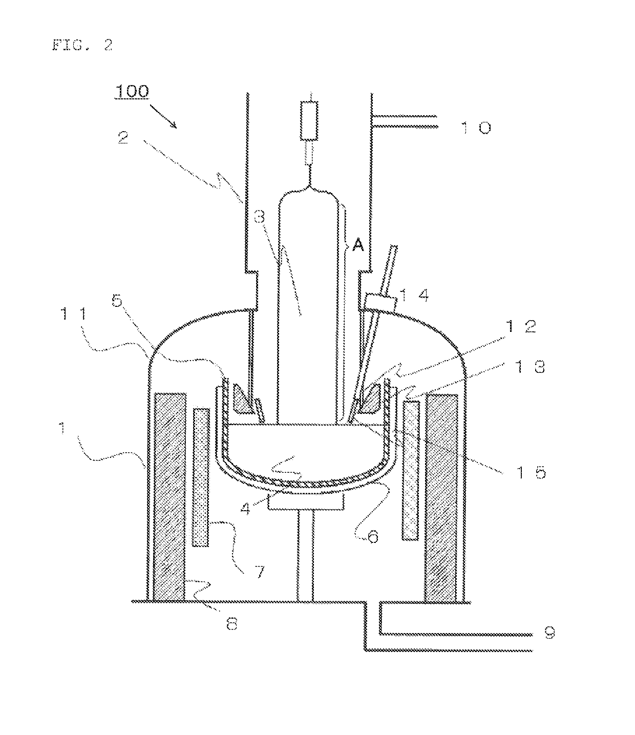
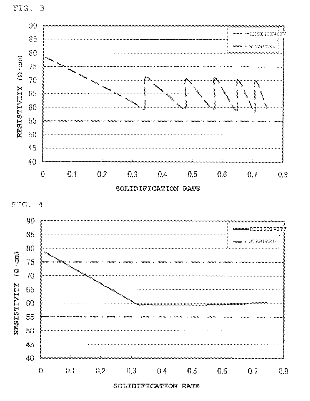
[0067]An n-type silicon single crystal having a resistivity standard of 55-75 Ω·cm and a diameter of 200 mm was grown with the CZ single crystal growth apparatus 100 shown in FIG. 2. The initial charge amount of silicon raw materials was 200 kg, and about 160 kg of a silicon single crystal was grown. Considering a single crystal top portion inferior in qualities other than resistivity (e.g., oxygen concentration or the like), initial doping was carried out by using phosphorus (P) as the primary dopant such that the resistivity reached the standard when the straight body portion had a length of about 20 cm from the top of the straight body portion and the solidification rate became about 0.09. In regard to the doping amount, 0.82 g of a doping agent prepared by pulverizing a silicon single crystal having a phosphorus concentration of 4×10¹⁹ atoms / cm3 was used. This doping amount allows the crystal to satisfy the resistivity standard up to a straight body portion length of about 100 c...

example 2

[0070]After the crystal of Example 1 was grown, about 160 kg of a silicon raw material was additionally fed so as to give a total raw material weight of 200 kg. For growing the second silicon single crystal, an n-type silicon single crystal having a resistivity standard of 55-75 Ω·cm and a diameter of 200 mm was grown. Calculations showed that the phosphorus (P) concentration remaining in the raw material melt 4 after completion of growth of the first silicon single crystal was 1.7×10¹⁴ atoms / cm3, and the boron (B) concentration remaining in the raw material melt 4 after completion of growth of the first silicon single crystal was 6.7×10¹³ atoms / cm3. Considering these residues, 0.79 g of a doping agent obtained by pulverizing a silicon crystal having a phosphorus (P) concentration of 4×10¹⁹ atoms / cm3 was introduced to prepare a raw material melt for growing the second silicon single crystal such that the resistivity reached the standard when the straight body portion had a length of...


PUM

PropertyMeasurementUnit
resistivityaaaaaaaaaa
diameteraaaaaaaaaa
resistivityaaaaaaaaaa

Abstract

A method controls a resistivity of a grown silicon single crystal by using a dopant when the silicon single crystal is grown by CZ method, including the steps of initially doping with a primary dopant such that the silicon single crystal has a predetermined conductive type and additionally doping with a secondary dopant having a conductive type opposite to that of the primary dopant continuously or intermittently, according to a solidification rate expressed by (crystalized weight) / (initial weight of silicon raw material) while growing the silicon single crystal, wherein in the additional doping step, the additional doping with the secondary dopant is carried out when the solidification rate is a predetermined value .alpha. or more, while the crystal is not doped with the secondary dopant until the solidification rate reaches the predetermined value .alpha..

Description

TECHNICAL FIELD[0001]The present invention relates to a method for controlling a resistivity of a silicon single crystal grown by the CZ method and an n-type silicon single crystal having a resistivity controlled by the method for controlling a resistivity.BACKGROUND ART[0002]An n-type crystal is mainly used in switching devices for power application such as IGBT (insulated gate bipolar transistor) or the like. Conventionally, EPW (an epitaxial wafer) and FZ-PW (a wafer produced by the FZ method), whose resistivity can be relatively easily controlled, have been used. Unfortunately, EPW is expensive since an additional step (an epitaxial growth step) is included compared with CZ-PW (a wafer produced by the CZ method), and the FZ method has a difficulty in increasing a crystal diameter. Therefore, use of CZ-PW on which no epitaxial layer is stacked has attracted attention. However, a silicon single crystal produced by the CZ method causes a segregation phenomenon, so that it is diffic...

Claims


Application Information

Patent Timeline
Patent Type & Authority Patents(United States)
IPC IPC(8): C30B15/04C30B15/20C30B29/06H01L29/739H01L29/167
CPCC30B15/04H01L29/167H01L29/7393C30B15/20C30B29/06
Inventor HOSHI, RYOJIKAMADA, HIROYUKITAKANO, KIYOTAKA
Owner SHIN-ETSU HANDOTAI CO LTD
Why Eureka
Try Eureka