Separation of workpiece with three material removal stages

a technology of separation and removal stages, applied in the direction of fine working devices, electrical equipment, and testing/measurement of semiconductor/solid-state devices, can solve the problems of reducing the reliability of the manufactured die, cracks on the front side, etc., and achieve the effect of suppressing the separation artefacts

a technology of separation and removal stages, applied in the direction of fine working devices, electrical equipment, and testing/measurement of semiconductor/solid-state devices, can solve the problems of reducing the reliability of the manufactured die, cracks on the front side, etc., and achieve the effect of suppressing the separation artefacts

US10403506B2Active Publication Date: 2019-09-03INFINEON TECH AG

Image

  • Separation of workpiece with three material removal stages
  • Separation of workpiece with three material removal stages
  • Separation of workpiece with three material removal stages

Examples


Embodiment Construction

[0010]In the following, further exemplary embodiments of the apparatus and the methods will be explained.

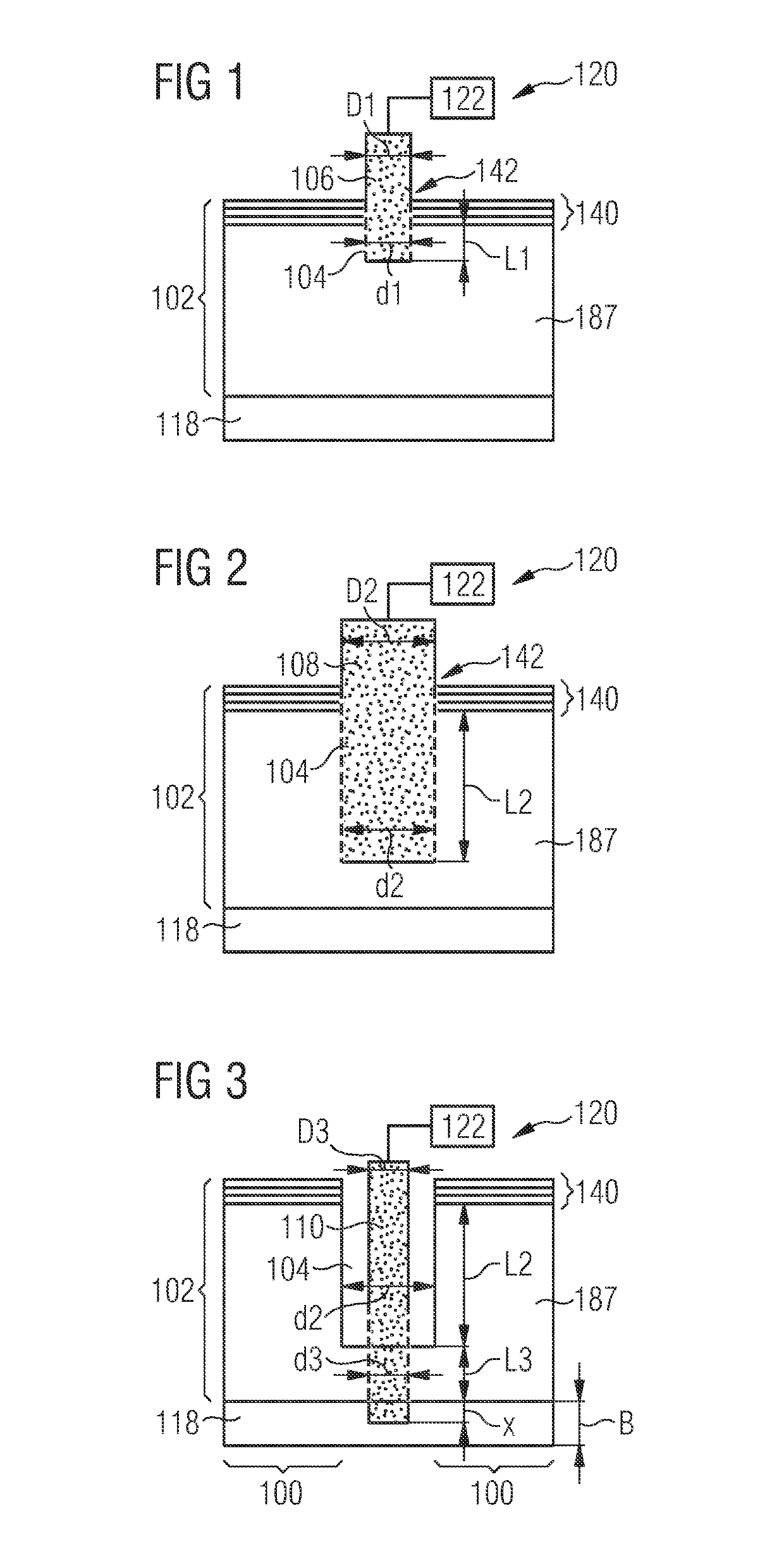
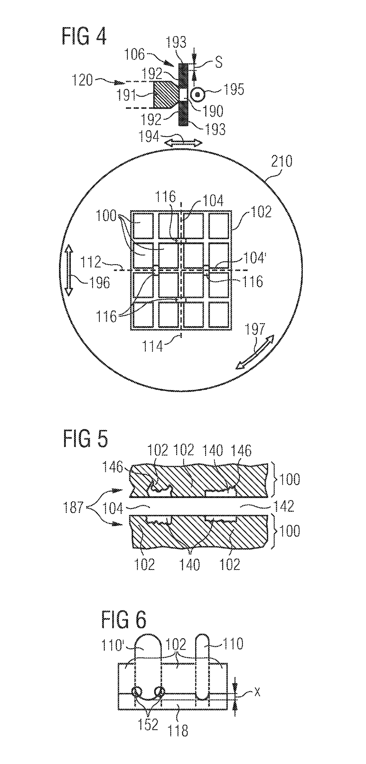
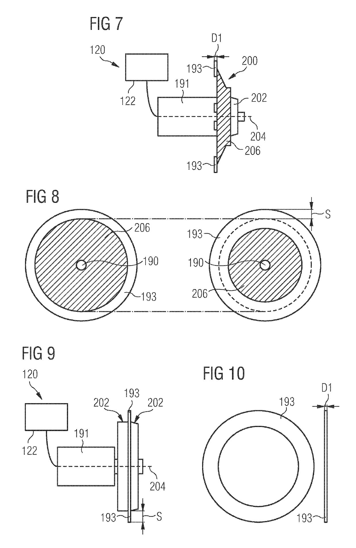
[0011]In the context of the present application, the term “workpiece” may denote one single integrally formed body. One example for an integral workpiece is a semiconductor wafer before singularization in its electronic dies. Another example for an integral workpiece is a semiconductor wafer which is already partially singularized into its individual separate electronic dies, wherein however the electronic dies are integrally held together by a common carrier (in particular having an adhesive surface) on which the electronic dies are fixedly mounted. Such a carrier may for instance be a carrier tape or a carrier plate (for example made of glass or silicon) on which the individual electronic dies may be fixedly attached.

[0012]In the context of the present application, the term “wafer” may particularly denote a flat slice of semiconductor material, such as a crystalline silicon, us...


PUM


Abstract

A method of manufacturing electronic dies by separating a wafer into electronic dies, wherein the method comprises forming a groove in the wafer with a first material removal tool having a first thickness, enlarging the groove by a second material removal tool having a second thickness larger than the first thickness, and subsequently increasing a depth of the groove by a third material removal tool having a third thickness smaller than the second thickness until the wafer is separated.

Description

BACKGROUND OF THE INVENTIONField of the Invention[0001]The present invention relates to a method of manufacturing electronic dies by separating a wafer into electronic dies, a method for singulating dies, a method of separating a workpiece into separate sections, and an apparatus for separating a wafer into electronic dies.Description of the Related Art[0002]Packages may be denoted as encapsulated electronic dies with electrical connects extending out of the encapsulant and being mounted to an electronic periphery, for instance on a printed circuit board. Before packaging the electronic dies, a semiconductor wafer is singularized into a plurality of electronic dies. One or more of the electronic dies may then be encapsulated in an encapsulant of the package.[0003]Singularization of a semiconductor wafer is accomplished in many cases by sawing the wafer mechanically into separate electronic dies. However, this may conventionally involve issues such as layer delamination, chipping or ...

Claims


Application Information

Patent Timeline
03 Sep 2019
Publication
US10403506B2
IPC
H01L21/304; H01L21/78; H01L21/67; H01L21/66
CPC
H01L21/78; H01L21/3043; H01L21/67092; H01L22/34; B28D5/022
Inventors
KAMSEDER, CHRISTOPH; MARIANI, FRANCO