Supercharge Your Innovation With Domain-Expert AI Agents!

Method for manufacturing CMOS structure

a technology of complementary metal oxide and semiconductor, applied in the field of semiconductor technology, can solve the problems of poor reliability of products, increase manufacturing costs, and low yield, and achieve the effect of reducing reliability problems and reducing manufacturing costs of a cmos process

Active Publication Date: 2019-10-08
SILERGY SEMICON TECH (HANGZHOU) CO LTD
View PDF9 Cites 0 Cited by
  • Summary
  • Abstract
  • Description
  • Claims
  • Application Information

AI Technical Summary

Benefits of technology

The present invention is a method for making a semiconductor structure by overdoping a specific region of a lightly-doped region with the same type of dopants. This helps to compensate for the lack of dopants in the region. Only one mask is used for both types of MOSFETs when forming the lightly-doped regions, reducing the number of masks and avoiding failures in the structure due to mismatches between different masks. The technical effect is an improved method for making semiconductor structures that results in better performance and reliability.

Problems solved by technology

Consequently, a large number of masks must be used in various doping steps in the conventional CMOS process, which increases manufacturing cost, and may cause low yield and poor reliability of the product due to possible mismatching of different masks.

Method used


Image

  • Method for manufacturing CMOS structure
  • Method for manufacturing CMOS structure
  • Method for manufacturing CMOS structure

Examples


Embodiment Construction

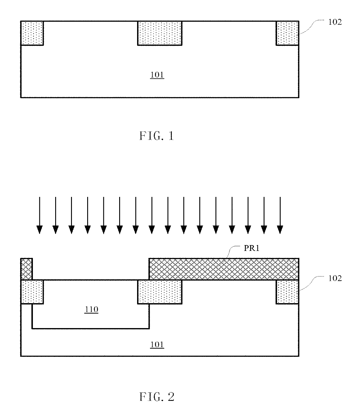
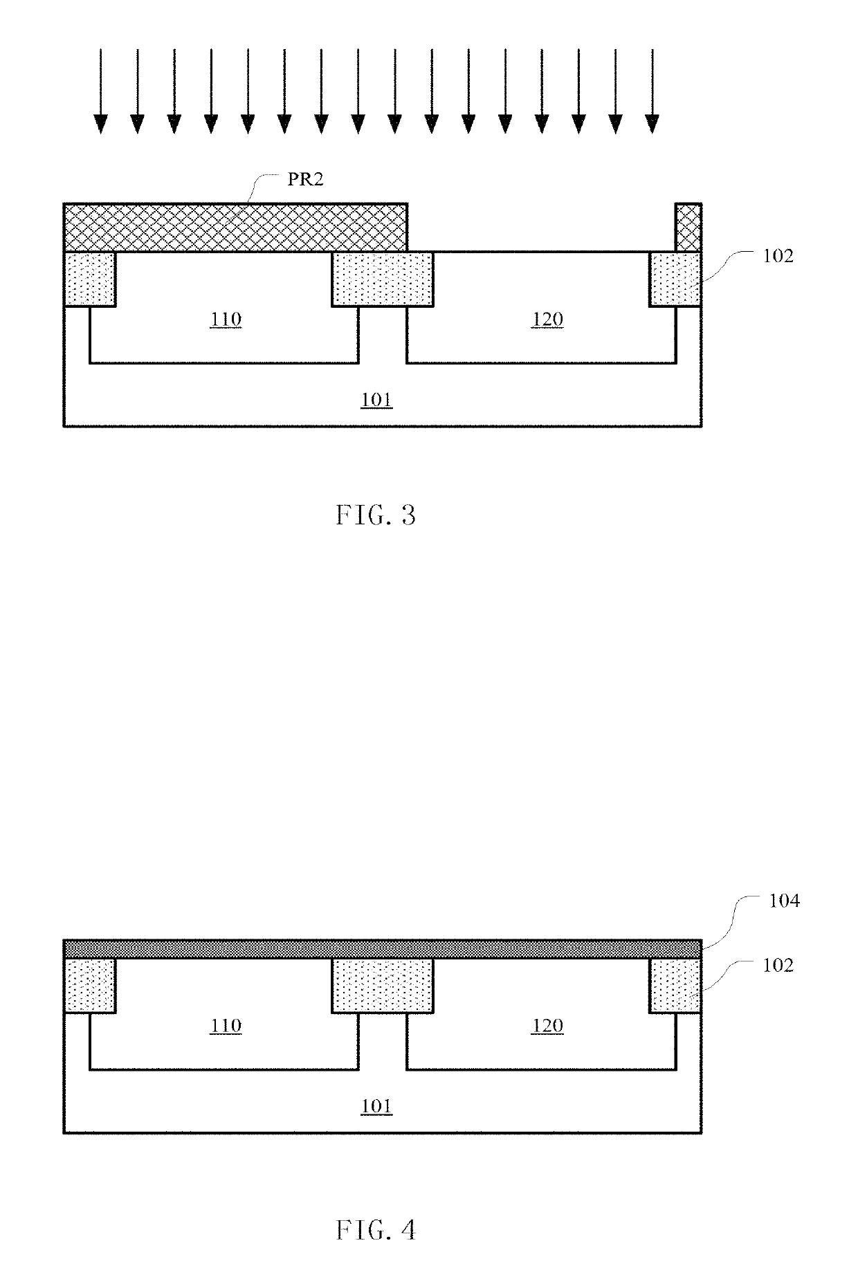
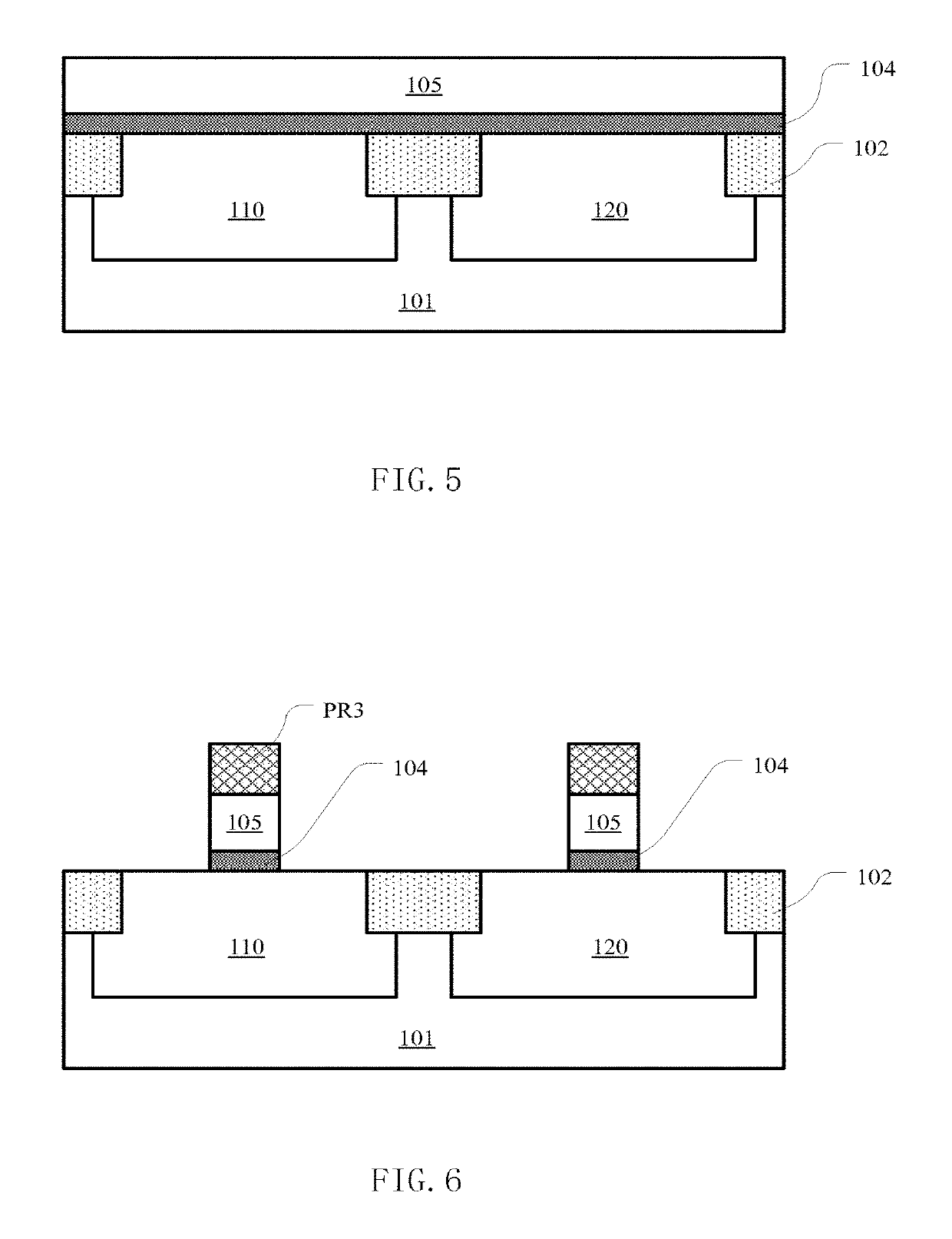
[0029]Exemplary embodiments of the present disclosure will be described in more details below with reference to the accompanying drawings. In the drawings, like reference numerals denote like members. The figures are not drawn to scale, for the sake of clarity. Moreover, some well-known parts may not be shown. For simplicity, the structure of the semiconductor device having been subject to several relevant process steps may be shown in one figure.

[0030]It should be understood that when one layer or region is referred to as being “above” or “on” another layer or region in the description of device structure, it can be directly above or on the other layer or region, or other layers or regions may be intervened therebetween. Moreover, if the device in the figures is turned over, the layer or region will be “under” or “below” the other layer or region.

[0031]In contrast, when one layer is referred to as being “directly on” or “on and adjacent to” or “adjoin” another layer or region, ther...


PUM


Abstract

The present disclosure relates to a method for manufacturing a CMOS structure. A first gate stack is formed on a semiconductor substrate in a first region. A second gate stack is formed on the semiconductor substrate in a second region. A dopant of a first type is implanted with the first gate stack and the second gate stack as a hard mask to form a lightly-doped drain region of the first type. A dopant of a second type is implanted by using a first mask and with the second gate stack as a hard mask to form a lightly-doped drain region of the second type. The first mask blocks the first region and exposes the second region. When the lightly-doped drain region of the second type is formed, the dopant of the second type over dopes a predetermined region of the lightly-doped drain region of the first type.

Description

CLAIM OF PRIORITY[0001]This application is a continuation of the following application, U.S. patent application Ser. No. 14 / 823,058, filed on Aug. 11, 2015, and which is hereby incorporated by reference as if it is set forth in full in this specification, and which also claims priority to Chinese Application No. 201410392572.9, filed Aug. 11, 2014 (not published), and claims priority to Chinese Application No. 201410456374.4, filed Sep. 9, 2014 (published as CN 104167391 A), both of which are hereby incorporated by reference.BACKGROUND OF THE DISCLOSURE[0002]Field of the Disclosure[0003]The present disclosure relates to semiconductor technology, and more particularly, to a method for manufacturing a complementary metal oxide semiconductor (CMOS) structure.[0004]Description of the Related Art[0005]A CMOS structure includes metal-oxide-semiconductor field-effect transistors (MOSFETs) of two opposite types (i.e. N-type and P-type) on one semiconductor substrate. The CMOS structure is w...

Claims


Application Information

Patent Timeline
Patent Type & Authority Patents(United States)
IPC IPC(8): H01L21/82H01L21/265H01L21/8238H01L29/66
CPCH01L21/823814H01L21/26593H01L21/823842H01L21/8238H01L29/66803H01L21/823828
Inventor YOU, BUDONGLYU, ZHENGHUANG, XIANGUOPENG, CHUAN
Owner SILERGY SEMICON TECH (HANGZHOU) CO LTD
Features
  • R&D
  • Intellectual Property
  • Life Sciences
  • Materials
  • Tech Scout
  • Unparalleled Data Quality
  • Higher Quality Content
  • 60% Fewer Hallucinations
Learn More