Touch sensing high-low driving scheme for in-cell touch LCD display
a high-low driving scheme and touch sensing technology, applied in the field of touch sensing techniques and mechanisms, can solve the problems of large parasitic capacitance build-up, affecting the signal-to-noise ratio (snr) of touch sensing signals, parasitic capacitance build-up on touch sensors, etc., to mitigate certain imperfections and eliminate parasitic capacitance
- Summary
- Abstract
- Description
- Claims
- Application Information
AI Technical Summary
Benefits of technology
Problems solved by technology
Method used
Image
Examples
first embodiment
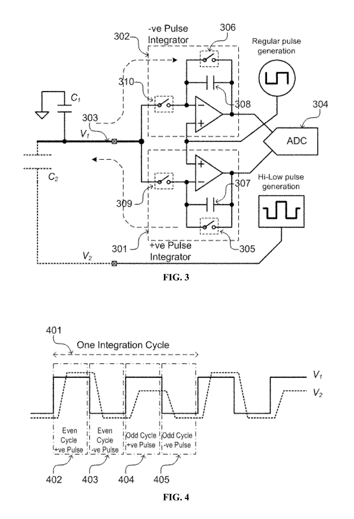
[0041]FIG. 3 depicts the circuit diagram illustrating the touch analog frontend (TAFE) design and touch-sensing signal-driving scheme in accordance to a first embodiment of the present invention. Only a single sense channel and TAFE circuitry is shown in FIG. 3 for clarity. In a legitimate implementation, multiple sense channels and TAFE circuitries are deployed in parallel. During a touch-sensing period of the touch-display panel operation, a sensor electrode regular excitation signal V1 is provided for driving a sensor electrode, wherein V1 is a square wave signal, in which the amplitude alternates periodically between a maximum value and a minimum value. The positive going transitions and the negative going transitions of V1 have substantially similar slopes. In real-life applications, multiple sense channels are driven by multiple sensor electrode regular excitation signals simultaneously. Each of the sensor electrode regular excitation signals is generated by an active integrat...
second embodiment
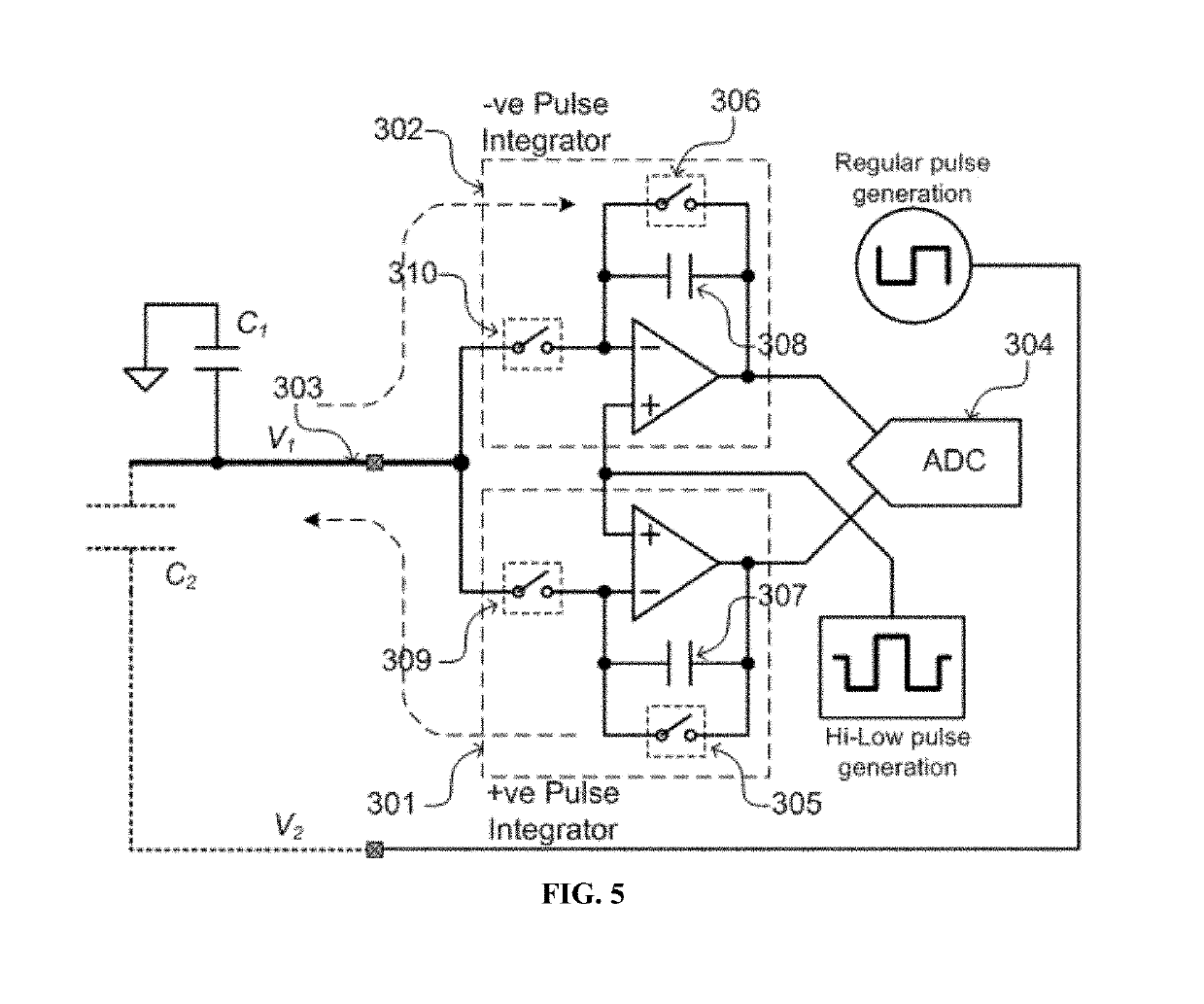
[0059]FIG. 5 depicts the circuit diagram illustrating the TAFE design and touch-sensing signal-driving scheme in accordance to a second embodiment of the present invention. Again only a single sense channel and TAFE circuitry is shown in FIG. 5 for clarity. In a legitimate implementation, multiple sense channels and TAFE circuitries are deployed in parallel. In this second embodiment, during a touch-sensing period of the touch-display panel operation, an embedded electrodes regular excitation signal V2 is provided for driving the embedded electrodes, wherein V2 is a square wave signal, in which the amplitude alternates periodically between a maximum value and a minimum value. The positive going transitions and the negative going transitions of V2 have substantially similar slopes.
[0060]In addition, a sensor electrode high-low excitation signal V1 is provided for indirectly driving the sensor electrodes, wherein V1 is similar to the embedded electrodes regular excitation signal V2 ex...
third embodiment
[0076]Referring to FIG. 7. In a third embodiment, a touch-sensing signal-driving scheme that is the same as that in the first embodiment is provided. The TAFE design in this third embodiment, however, uses only a positive pulse integrator 701 connected in series with each sensor electrode. This TAFE design is simpler than that of the first embodiment. This provides the advantages of lower manufacturing cost and die space savings. On the other hand, the single positive pulse integrator 701 output as a single-end input to the ADC would have poorer SNR than the combined positive and negative pulse integrator outputs as a differential input to the ADC.
PUM
| Property | Measurement | Unit |
|---|---|---|
| parasitic capacitance | aaaaa | aaaaa |
| parasitic capacitance | aaaaa | aaaaa |
| frequencies | aaaaa | aaaaa |
Abstract
Description
Claims
Application Information


