Directional coupler and wireless communication device using the same
a wireless communication device and directional coupler technology, applied in the direction of waveguide type devices, antenna earthings, gain control, etc., can solve the problems of increasing the chip size, manufacturing irregularities, and increasing the loss of sub lines, so as to reduce the chip size, small chip size, and satisfactory characteristics
- Summary
- Abstract
- Description
- Claims
- Application Information
AI Technical Summary
Benefits of technology
Problems solved by technology
Method used
Image

Examples
first embodiment
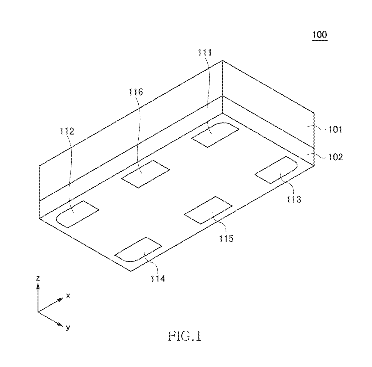
[0048]FIG. 1 is a schematic perspective view illustrating the outer appearance of a directional coupler 100 according to the first embodiment of the present invention.
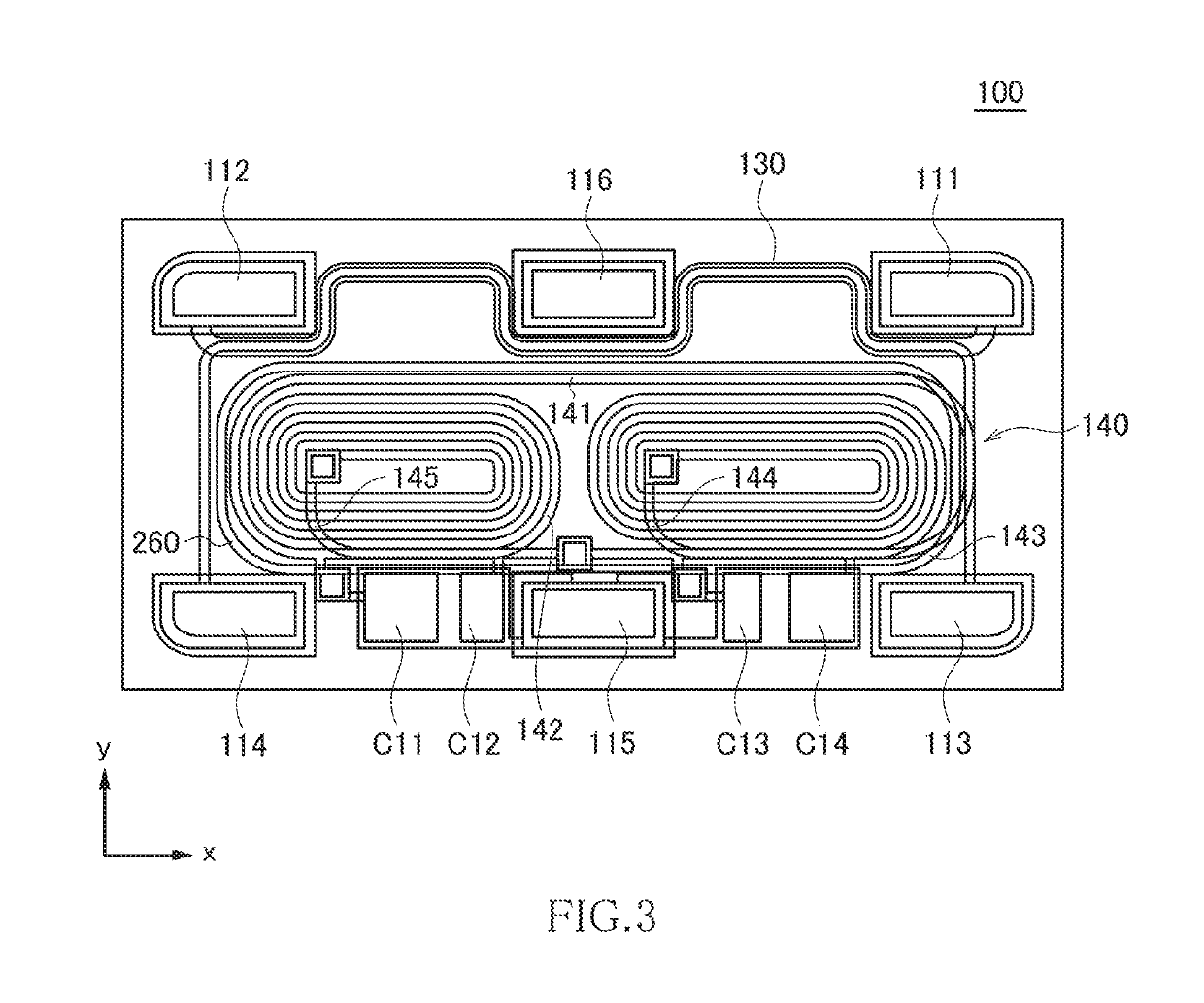
[0049]As illustrated in FIG. 1, the directional coupler 100 according to the present embodiment is a chip component having a substantially rectangular parallelepiped shape and has a structure in which a laminated structure 102 is formed on a substrate 101. In FIG. 1, the laminated structure 102 of the directional coupler 100 facing downward is viewed from obliquely below. Although not particularly limited, the length of the directional coupler 100 in the x-direction is 1.0 mm, the width thereof in the y-direction is 0.5 mm, and the height thereof in the z-direction is 0.3 mm. The substrate 101 is made of, e.g., a non-magnetic material such as ferrite, serves as a support for forming the laminated structure 102, and plays a role of ensuring mechanical strength of the directional coupler 100.
[0050]The laminated structure...
second embodiment
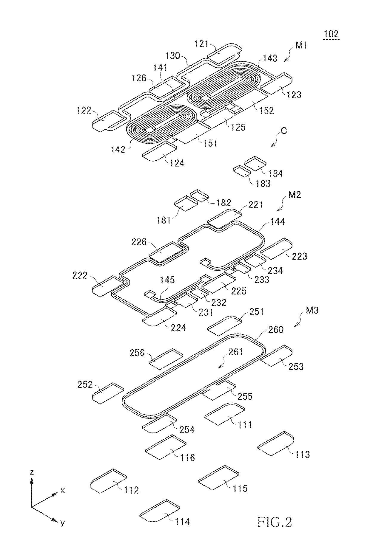
[0085]FIG. 16 is a view for explaining the structure of a directional coupler 300 according to a second embodiment of the present invention and is a see-through view of a conductor layer included in the laminated structure 102 as viewed in the lamination direction (z-direction). FIGS. 17 to 24 are plan views each illustrating the configuration of each layer constituting the laminated structure 102. The directional coupler 300 according to the second embodiment has the same outer appearance as that of the directional coupler 100 of FIG. 1 according to the first embodiment and has the terminal electrodes 111 to 116 on its bottom surface.
[0086]As illustrated in FIGS. 16 to 24, like the first embodiment, the laminated structure 102 constituting the directional coupler 300 according to the present embodiment is constituted of the conductor layers M1 to M3, capacitor electrode layers C, and insulating layers I1 to I4 provided between the adjacent conductor layers or adjacent conductor and...
third embodiment
[0115]FIG. 28 is a block diagram of a wireless communication device 500 using the directional coupler 100 or directional coupler 300.
[0116]The wireless communication device 500 illustrated in FIG. 28 includes an antenna 501, a power amplifier 502 that supplies a transmission signal to the antenna 501, an automatic output control circuit 503 that adjusts the gain of the power amplifier 502, and the above-described directional coupler 100 or directional coupler 300 connected between the antenna 501 and the power amplifier 502. Specifically, the terminal electrode 111 and the terminal electrode 112 of the directional coupler 100 or 300 are connected to the power amplifier 502 and the antenna 501, respectively. In this configuration, a transmission signal supplied from the power amplifier 502 is transmitted to the antenna 501 by way of the main line of the directional coupler 100 or 300.
[0117]The terminal electrode 113 of the directional coupler 100 or directional coupler 300 is connect...
PUM
 Abstract
Description
Claims
Application Information
 - R&D
- Intellectual Property
- Life Sciences
- Materials
- Tech Scout
- Unparalleled Data Quality
- Higher Quality Content
- 60% Fewer Hallucinations
Browse by: Latest US Patents, China's latest patents, Technical Efficacy Thesaurus, Application Domain, Technology Topic, Popular Technical Reports.
© 2025 PatSnap. All rights reserved.Legal|Privacy policy|Modern Slavery Act Transparency Statement|Sitemap|About US| Contact US: help@patsnap.com