Semiconductor device with bus terminating function

a technology of a semiconductor device and a bus, applied in the field of semiconductor devices, can solve the problems of low reliability, signal cannot be transmitted at high speed, and electrical static damage, and achieve the effects of high speed, accurate transmission of signals, and high speed

Inactive Publication Date: 2006-02-02
RENESAS ELECTRONICS CORP
View PDF31 Cites 1 Cited by
  • Summary
  • Abstract
  • Description
  • Claims
  • Application Information

AI Technical Summary

Benefits of technology

[0015] An object of the present invention is to provide a semiconductor device capable of transferring a signal accurately at high speed, without increase in circuit area and degradation in reliability.
[0016] Another object of the present invention is to provide a semiconductor circuit device with an output circuit containing a terminating circuit, which is capable of transferring a signal of CMOS level at high speed with small occupying area and high reliability.
[0018] By arranging the terminating circuit inside the semiconductor device, a signal can be transmitted through selective operation of the terminating circuit while maintaining the impedance matching to the bus, even when the system configuration is modified. Therefore, a signal can be transmitted at high speed with no adverse effect by an interconnection line impedance or others.
[0019] Additionally, by setting the drain contact-to-gate (control electrode) length in the terminating transistor shorter than in the output transistor, the area will not be increased despite of placing the terminating circuit. Further, by placing the terminating resistance element, the breakdown voltage against the surge of the terminating transistor can be assured. Thus, a reliable semiconductor device with a small occupying area, having an output circuit that is capable of transmitting a signal at high speed can be implemented.

Problems solved by technology

However, in an MOS output circuit configured with an MOS transistor, a large current may flow into the output transistor or high electric field may be generated at drain due to the surge voltage, which may result in electrostatic damage.
If the drain diffusion resistance functions as terminating resistance, then an output signal is driven via high drain diffusion resistance in signal outputting, and thus the signal can not be transmitted at high speed.
Consequently, the parasitic capacitance of the output pin terminal increases, and thus, a signal can not be transmitted at high speed.
Further, since the terminating resistance element is connected between the drain of the output transistor and the output pad and functions as a current limiting element for an output signal, the signal can not be output at high speed.
Moreover, since the terminating resistance causes a voltage drop, a signal at CMOS level can not be transmitted.

Method used


Image

  • Semiconductor device with bus terminating function
  • Semiconductor device with bus terminating function
  • Semiconductor device with bus terminating function

Examples


first embodiment

[0038] First Embodiment

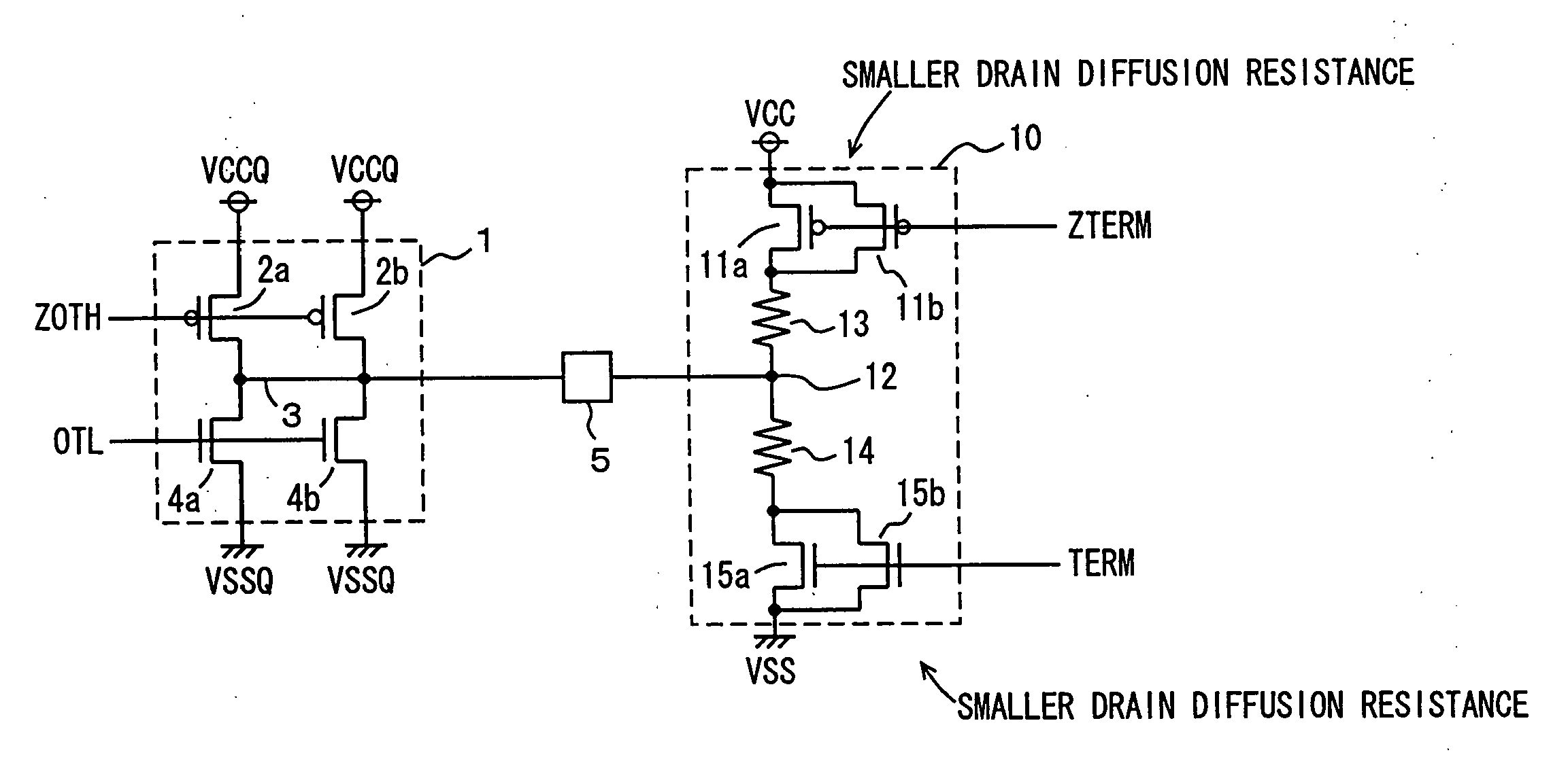
[0039]FIG. 1 shows a configuration of a main part of a semiconductor device according to a first embodiment of the present invention. In FIG. 1, an output circuit 1 and a terminating circuit 10 provided for an external output pad 5 are representatively shown. Pad 5 is connected to a pin terminal, which is not shown.

[0040] Output circuit 1 includes P-channel MOS transistors 2a and 2b each connected between a power supply node and an output node 3 and selectively made conductive in accordance with an output control signal ZOTH, and N-channel MOS transistors 4a and 4b each connected between output node 3 and a ground node and selectively made conductive in accordance with an output control signal OTL. Power supply voltage VCCQ for the output circuit is supplied to the power supply node, and ground voltage VSSQ for the output circuit is supplied to the ground node. Output node 3 is connected to output pad 5.

[0041] The logic levels of output control signals ZOTH ...

first modification

[0071] First Modification

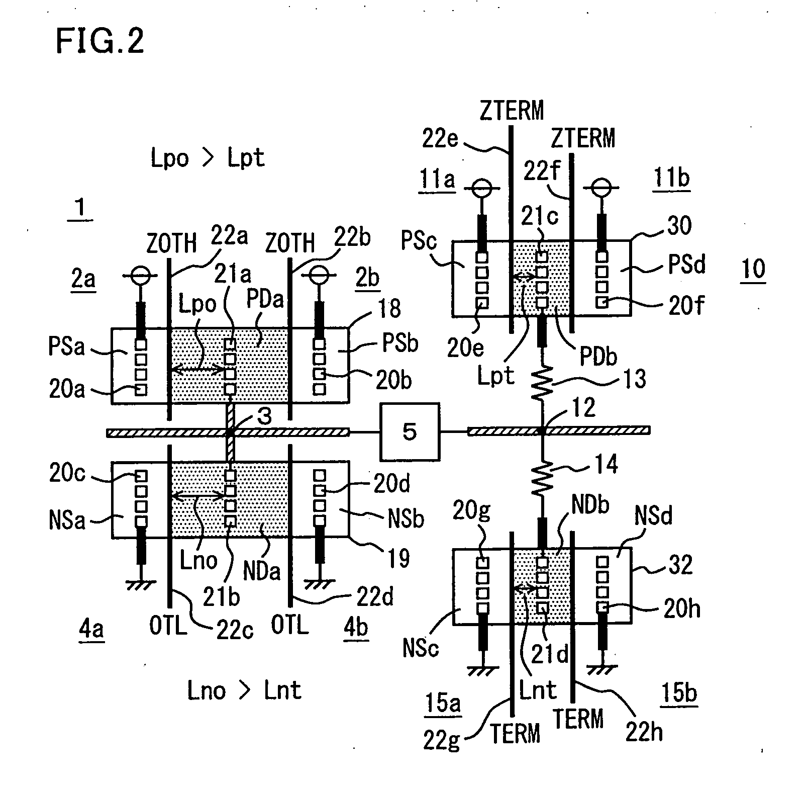
[0072]FIG. 3 schematically shows a layout of transistors in output circuit 1 and terminating circuit 10 according to a first modification of the first embodiment of the present invention. The layout of the semiconductor circuit device shown in FIG. 3 is different from that of FIG. 2 in the following points. No pulling-down termination circuit portion is provided in terminating circuit 10. Terminating resistance element 13 and P-type active region 30 forming P-channel MOS transistors 11a and 11b are provided. In P-type active region 30, the distances Lpt from drain contact 21c to gate electrode 22e and to gate electrode 22f, respectively, are set sufficiently shorter as compared with the corresponding distance Lpo of P-channel MOS transistors included in output circuit 1. In this case, the distance Lpt is set shorter than the drain contact-to-gate electrode distance Lno of N-channel MOS transistors of output circuit 1.

[0073] The other configuration of the ci...

second modification

[0081] Second Modification

[0082]FIG. 5 schematically shows the layout of an output circuit and a terminating circuit according to a second modification of the first embodiment of the present invention. The layout shown in FIG. 5 is different from the layout shown in FIG. 2 in the following points. P-type active region 18 is not arranged, but an N-type active region 19 is arranged in output circuit 1. The distance between drain contact 21b and gate electrode 22c in N-type active region 19 is set to Lno. Source impurity regions NSa and NSb are coupled to ground nodes via source contacts 20c and 20d, respectively.

[0083] In output circuit 1, MOS transistors 4a and 4b are arranged to drive output node 3 in accordance with output control signal OTL applied to gate electrodes 22c and 22d. Accordingly, the output circuit 1 drives the external signal line via output pad 5, according to the open-drain scheme.

[0084] The configuration of terminating circuit 10 is similar to the layout of term...


PUM


Abstract

The distance between a drain contact and gate electrode in a terminating transistor, which couples a termination resistor connected to an output terminal to a power source node, is set shorter than in an output transistor, which drives an output-node in accordance with an internal signal. The area of the terminating circuit is reduced while the reliability against the surge is maintained. Thus, an output circuit containing the terminating circuit that occupies a small area and is capable of transmitting a signal / data at high speed is provided.

Description

RELATED APPLICATIONS [0001] This application is a continuation of application Ser. No. 10 / 391,021 filed Mar. 19, 2003, which claims priority of Japanese Application No. 2003-300891, filed Aug. 26, 2003, the contents of which are hereby incorporated by reference.BACKGROUND OF THE INVENTION [0002] 1. Field of the Invention [0003] The present invention relates to a semiconductor device driving an output node, and specifically, to a semiconductor device with a bus terminating function. [0004] 2. Description of the Background Art [0005] In a semiconductor device, a transistor connected to a pin terminal is easy to be affected by noises, since it is directly connected to the outside of the device via the pin terminal. Among the noises, one at a level enough to destruct a device (a transistor) is referred to as a surge. A destruction of a semiconductor device by the surge is referred to as electrostatic damage (ESD), which is accompanied by breakdown of a gate insulating film of an MOS tra...

Claims


Application Information

Patent Timeline
Patent Type & Authority Applications(United States)
IPC IPC(8): H03K19/003H01L21/822H01L21/8234H01L21/8238H01L27/04H01L27/06H01L27/088H01L27/092H04L25/02
CPCG06F13/4086H03K19/0005H04L25/0298H04L25/0278H04L25/028H03K19/00315
Inventor KUBO, TAKASHI
Owner RENESAS ELECTRONICS CORP
Why Eureka
Try Eureka