Semiconductor device with bus terminating function

a technology of a semiconductor device and a bus, applied in the field of semiconductor devices, can solve the problems of low reliability, signal cannot be transmitted at high speed, and electrical static damage, and achieve the effects of high speed, accurate transmission of signals, and high speed

Inactive Publication Date: 2006-01-26
RENESAS ELECTRONICS CORP
View PDF22 Cites 1 Cited by
  • Summary
  • Abstract
  • Description
  • Claims
  • Application Information

AI Technical Summary

Benefits of technology

[0015] An object of the present invention is to provide a semiconductor device capable of transferring a signal accurately at high speed, without increase in circuit area and degradation in reliability.

Problems solved by technology

However, in an MOS output circuit configured with an MOS transistor, a large current may flow into the output transistor or high electric field may be generated at drain due to the surge voltage, which may result in electrostatic damage. electrostatic damage, the resistance value of drain region (hereinafter referred to as a drain diffusion resistance) in the output transistor must be increased.
If the drain diffusion resistance functions as terminating resistance, then an output signal is driven via high drain diffusion resistance in signal outputting, and thus the signal can not be transmitted at high speed.
Consequently, the parasitic capacitance of the output pin terminal increases, and thus, a signal can not be transmitted at high speed.
Further, since the terminating resistance element is connected between the drain of the output transistor and the output pad and functions as a current limiting element for an output signal, the signal can not be output at high speed.
Moreover, since the terminating resistance causes a voltage drop, a signal at CMOS level can not be transmitted.

Method used


Image

  • Semiconductor device with bus terminating function
  • Semiconductor device with bus terminating function
  • Semiconductor device with bus terminating function

Examples


first embodiment

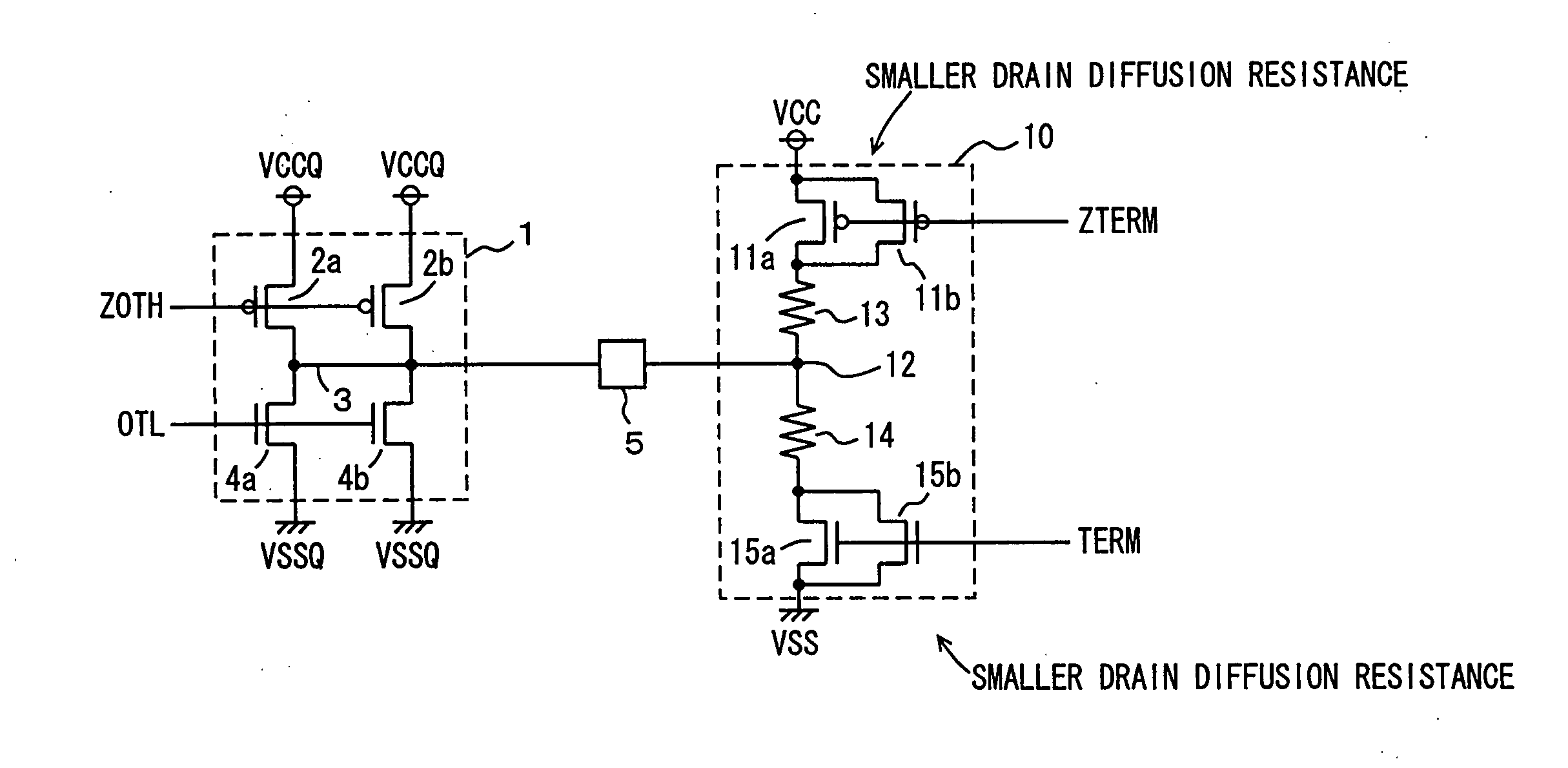
[0038]FIG. 1 shows a configuration of a main part of a semiconductor device according to a first embodiment of the present invention. In FIG. 1, an output circuit 1 and a terminating circuit 10 provided for an external output pad 5 are representatively shown. Pad 5 is connected to a pin terminal, which is not shown.

[0039] Output circuit 1 includes P-channel MOS transistors 2a and 2b each connected between a power supply node and an output node 3 and selectively made conductive in accordance with an output control signal ZOTH, and N-channel MOS transistors 4a and 4b each connected between output node 3 and a ground node and selectively made conductive in accordance with an output control signal OTL. Power supply voltage VCCQ for the output circuit is supplied to the power supply node, and ground voltage VSSQ for the output circuit is supplied to the ground node. Output node 3 is connected to output pad 5.

[0040] The logic levels of output control signals ZOTH and OTL are set in acco...

second embodiment

[0102]FIG. 9 schematically shows a configuration of an output circuit and a terminating circuit according to a second embodiment of the present invention (hereinafter, both of the circuits are collectively referred to as a semiconductor device). In the configuration shown in FIG. 9, output node 3 of output circuit 1 is electrically connected to pad 5 via interconnection line 50. Terminating circuit 10 is provided distant from pad 5 relative to output circuit 1. A terminating node 12 of terminating circuit 10 is connected to the same interconnection line 50. Terminating node 12 of terminating circuit 10 and output node 3 of output circuit 1 are electrically connected to pad 5 via common interconnection line 50.

[0103] Similarly to the first embodiment, output circuit 1 includes pulling up P-channel MOS transistors 2a and 2b, and pulling down N-channel MOS transistors 4a and 4b, which drive output node 3 in accordance with output control signals ZOTH and OTL, respectively.

[0104] Simi...


PUM


Abstract

The distance between a drain contact and gate electrode in a terminating transistor, which couples a termination resistor connected to an output terminal to a power source node, is set shorter than in an output transistor, which drives an output node in accordance with an internal signal. The area of the terminating circuit is reduced while the reliability against the surge is maintained. Thus, an output circuit containing the terminating circuit that occupies a small area and is capable of transmitting a signal/data at high speed is provided.

Description

RELATED APPLICATIONS [0001] This application is a continuation of application Ser. No. 10 / 391,021 filed Mar. 19, 2003, which claims priority of Japanese Application No. 2003-300891, filed Aug. 26, 2003, the contents of which are hereby incorporated by reference.BACKGROUND OF THE INVENTION [0002] 1. Field of the Invention [0003] The present invention relates to a semiconductor device driving an output node, and specifically, to a semiconductor device with a bus terminating function. [0004] 2. Description of the Background Art [0005] In a semiconductor device, a transistor connected to a pin terminal is easy to be affected by noises, since it is directly connected to the outside of the device via the pin terminal. Among the noises, one at a level enough to destruct a device (a transistor) is referred to as a surge. A destruction of a semiconductor device by the surge is referred to as electrostatic damage (ESD), which is accompanied by breakdown of a gate insulating film of an MOS tra...

Claims


Application Information

Patent Timeline
Patent Type & Authority Applications(United States)
IPC IPC(8): H03K19/003H01L21/822H01L21/8234H01L21/8238H01L27/04H01L27/06H01L27/088H01L27/092H04L25/02
CPCG06F13/4086H03K19/0005H04L25/0298H04L25/0278H04L25/028H03K19/00315
Inventor KUBO, TAKASHI
Owner RENESAS ELECTRONICS CORP
Why Eureka
Try Eureka