Method for designing arithmetic device allocation

a technology of arithmetic device and allocation method, which is applied in the direction of program control, computation using denominational number representation, instruments, etc., can solve the problems of preventing correct evaluation of logic synthesis steps, circuit malfunction, and increase power consumption, so as to minimize the increase in the circuit area, increase the total circuit area, and reduce the number of selectors

Inactive Publication Date: 2005-07-05
SHARP KK
View PDF11 Cites 6 Cited by
  • Summary
  • Abstract
  • Description
  • Claims
  • Application Information

AI Technical Summary

Benefits of technology

[0055]In the case where the arithmetic operation allocation is sequentially performed from an arithmetic operation using an arithmetic device having a small area, an arithmetic device having a large area has to be used at the end of the arithmetic operation allocation, thereby increasing the total circuit area. However, according to the method described above, as shown with respect to Embodiment 4 described below, it is possible to minimize an increase in a circuit area in the cases where an arithmetic device is added so as to reduce the number of selectors, prevent the generation of the loop including only a combination circuit, prevent the generation of a false path equal to or more than a designated period, or the like.
[0056]Thus, the invention described herein makes possible the advantages of providing an arithmetic device allocation design method capable of reducing circuit scale so as not to include a loop including only a combination circuit and a long false path in the circuit.

Problems solved by technology

Once the oscillation is caused, power consumption is increased and moreover, circuit operation becomes unstable, thereby causing circuit malfunction.
Furthermore, the presence of such a loop prevents correct evaluation of delays in the steps of logic synthesis, floor planning (layout by units of blocks), routing of layout (layout by units of a gate in a block), etc.
Therefore, the circuit created by the arithmetic device allocation design method for minimizing the number of arithmetic devices is unreliable.
If data flows through the path 176, a delay in the entire circuit becomes greater than the clock period of 100 ns, and therefore circuit malfunction is caused.
However, it is not possible to distinguish whether a path is a false path or a path through which data actually flows using an automatic logic synthesis tool, a floor planning tool, a layout routing tool, or the like which are presently available.
Therefore, a pseudo-timing error is caused because of the generation of a false path longer than a clock period, or an arithmetic device on the false path is replaced by an arithmetic device, which is fast but has a large area, at the time of the optimization in a logic synthesis step, so that a circuit area is increased for no reason.
If any tool capable of recognizing the false path is realized in the future, such problems would not be caused, but these problems are frequently caused at present.
However, this method detects a false path by performing a simulation so as to confirm that a timing error does not happen in reality, and therefore there is a problem that the detection of the false path requires a very long period of time.
Further, when there is any omission in simulation patterns, there is a possibility that a path through which a signal is actually transferred is mistakenly recognized as being a false path.

Method used


Image

  • Method for designing arithmetic device allocation
  • Method for designing arithmetic device allocation
  • Method for designing arithmetic device allocation

Examples


embodiment 1

(Embodiment 1)

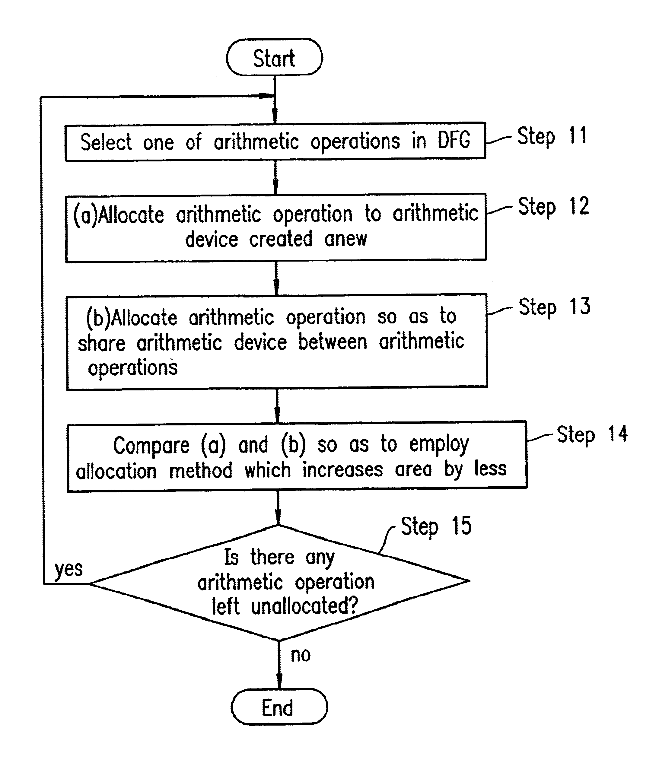
[0099]FIG. 16 is a flowchart for explaining an arithmetic device allocation design method according to Embodiment 1 of the present invention. In Embodiment 1, arithmetic operations in a data flow graph (DFG) are allocated to corresponding arithmetic devices one by one based on a scheduling result.

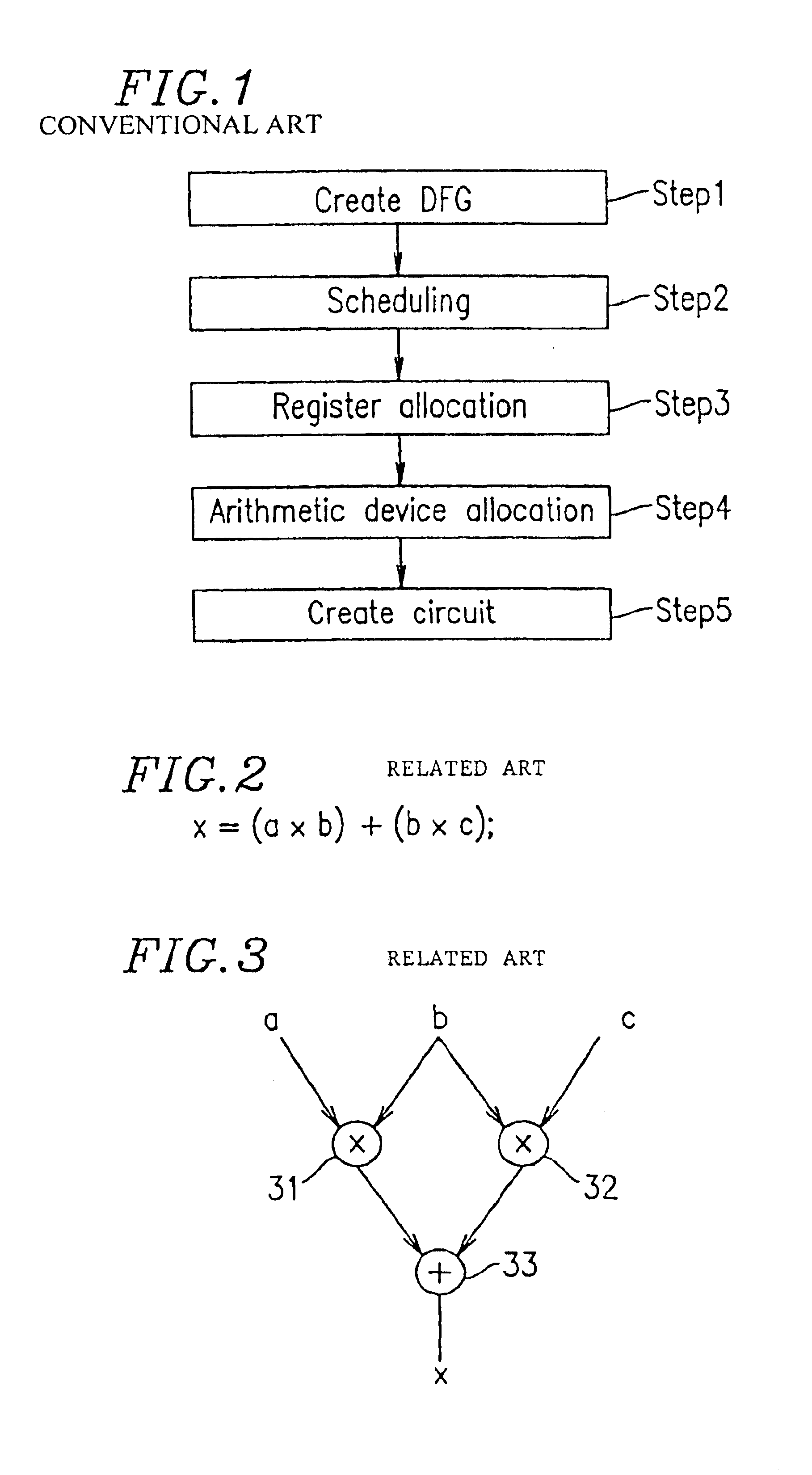
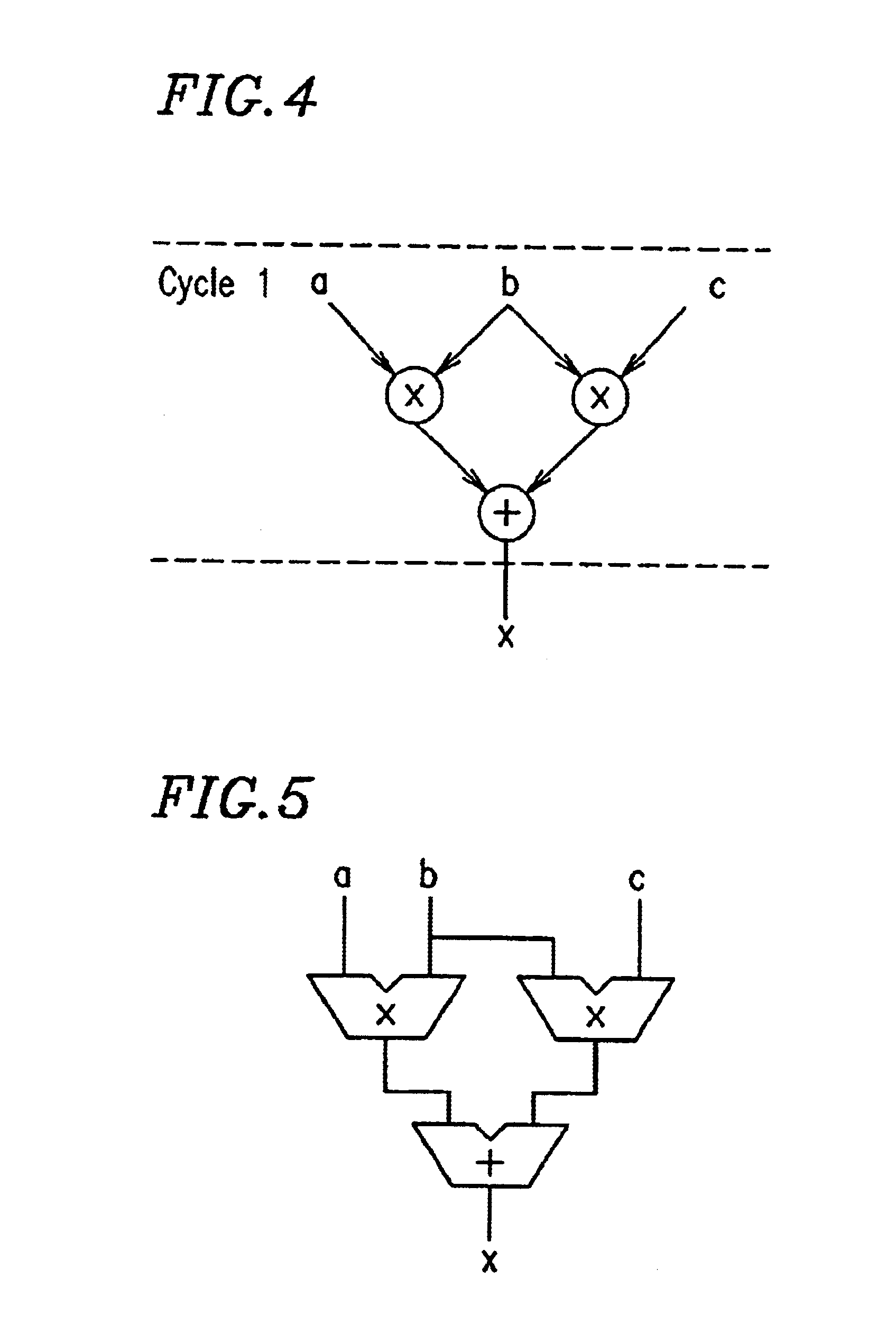
[0100]At step 11, one of the arithmetic operations in the DFG is selected. The following two methods (a) and (b) are respectively attempted at steps 12 and 13: (a) the arithmetic operation selected at step 11 is allocated to an arithmetic device created anew; and (b) an arithmetic operation is allocated to an arithmetic device to which another arithmetic operation has already been allocated so as to share the arithmetic device between these arithmetic operations. In such a case of allocating an arithmetic operation to an arithmetic device to which another operation has already been allocated so as to share the arithmetic device between these arithmetic operations, a selector i...

embodiment 2

(Embodiment 2)

[0119]FIG. 24 is a flowchart for explaining an arithmetic device allocation design method according to Embodiment 2. Embodiment 2 prevents the loop including only a combination circuit as shown in FIG. 13 from being generated when an arithmetic operation in the DFG is allocated to an arithmetic device based on a scheduling result.

[0120]Firstly, as a preparatory step, data dependency between arithmetic operations is examined according to a procedure as follows. At step 21, all the arithmetic operations to be allocated to arithmetic devices are detected from the DFG based on scheduling and register allocation results so as to be listed as focused arithmetic operations. Here, as shown in FIG. 25, each arithmetic device 141-144 is listed as a focused arithmetic operation based on, for example, the scheduling result of FIG. 12.

[0121]Next, at step 22, a pre-arithmetic operation or a post-arithmetic operation is determined with respect to each focused arithmetic operation. Th...

embodiment 3

(Embodiment 3)

[0136]FIG. 31 is a flow chart for explaining an arithmetic device allocation design method according to Embodiment 3. A false path refers to a path on which no operation is actually performed, and therefore no problems are caused to a circuit itself if the false circuit is present in the circuit. However, a conventional design verification tool cannot determine whether a path is a false path or a path on which any operation is actually performed, and thus detects the false path only as an error, thereby causing problems. Embodiment 3 prevents the generation of the false path causing a delay greater than a designated value when allocating the arithmetic operations to the arithmetic devices.

[0137]Firstly, when allocating a plurality of arithmetic operations to a single arithmetic device, it is checked whether or not a false path causing a delay is greater than a designated value.

[0138]At step 31 in FIG. 31, all the arithmetic operations to be allocated to an arithmetic d...


PUM


Abstract

An arithmetic device allocation design method of the present invention includes the steps of: in the case of allocating an arithmetic operation A to the arithmetic device, comparing an increased circuit area due to a selector to be provided so as to allocate the operation A to an arithmetic device C to which another arithmetic operation B has already been allocated and an increased area due to an arithmetic device D to be created anew to which only the operation A is allocated; when the increased circuit area due to the selector is smaller, allocating the operation A to the device C to which the another operation B has already been allocated while providing the selector; and when the increased circuit area due to the device D is smaller, creating the device D anew so as to allocate the operation A to the device D created anew.

Description

BACKGROUND OF THE INVENTION[0001]1. Field of the Invention[0002]The present invention relates to a method for designing arithmetic device allocation in which arithmetic operations in a data flow graph are allocated to arithmetic devices based on a scheduling result when performing high-level synthesis for automatically synthesizing a digital circuit from behavioral descriptions of an LSI circuit.[0003]2. Description of the Related Art[0004]Conventionally, high-level synthesis technologies are known as useful technologies for designing an LSI (Large Scale Integration) circuit in a short period of time. The high-level synthesis technologies are technologies for automatically synthesizing a circuit from behavioral descriptions which do not include information about a hardware structure and only includes a processing algorithm. For example, “High-Level Synthesis”, Kluwer Academic Publishers, is one publication including detailed description of conventional high-level synthesis technolog...

Claims


Application Information

Patent Timeline
Patent Type & Authority Patents(United States)
IPC IPC(8): G06F17/50G06F7/48
CPCG06F17/5045G06F7/48G06F30/30
Inventor OKADA, KAZUHISA
Owner SHARP KK
Why Eureka
Try Eureka