Operational amplifier and method of driving liquid crystal display
- Summary
- Abstract
- Description
- Claims
- Application Information
AI Technical Summary
Benefits of technology
Problems solved by technology
Method used
Image

Examples
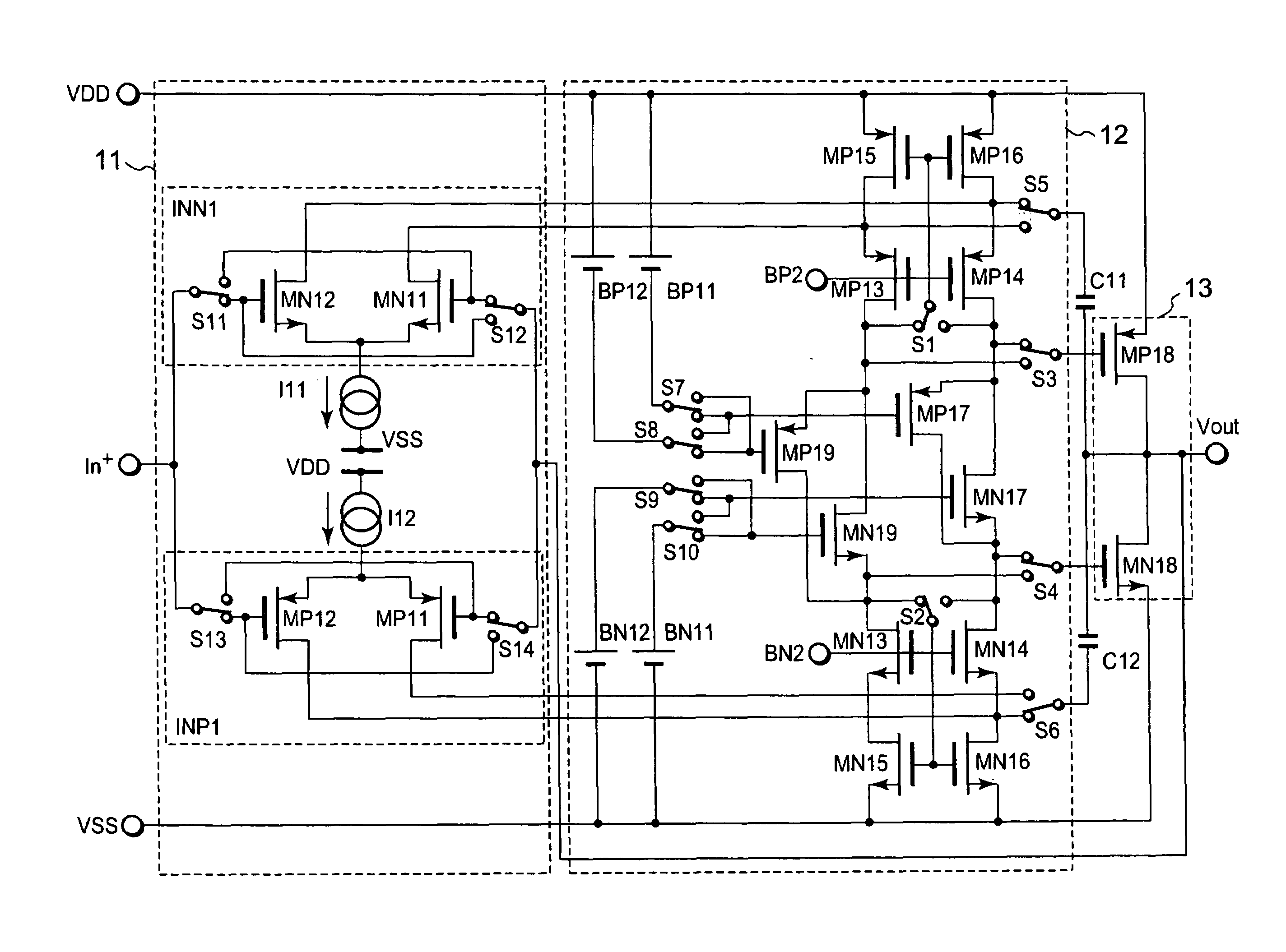
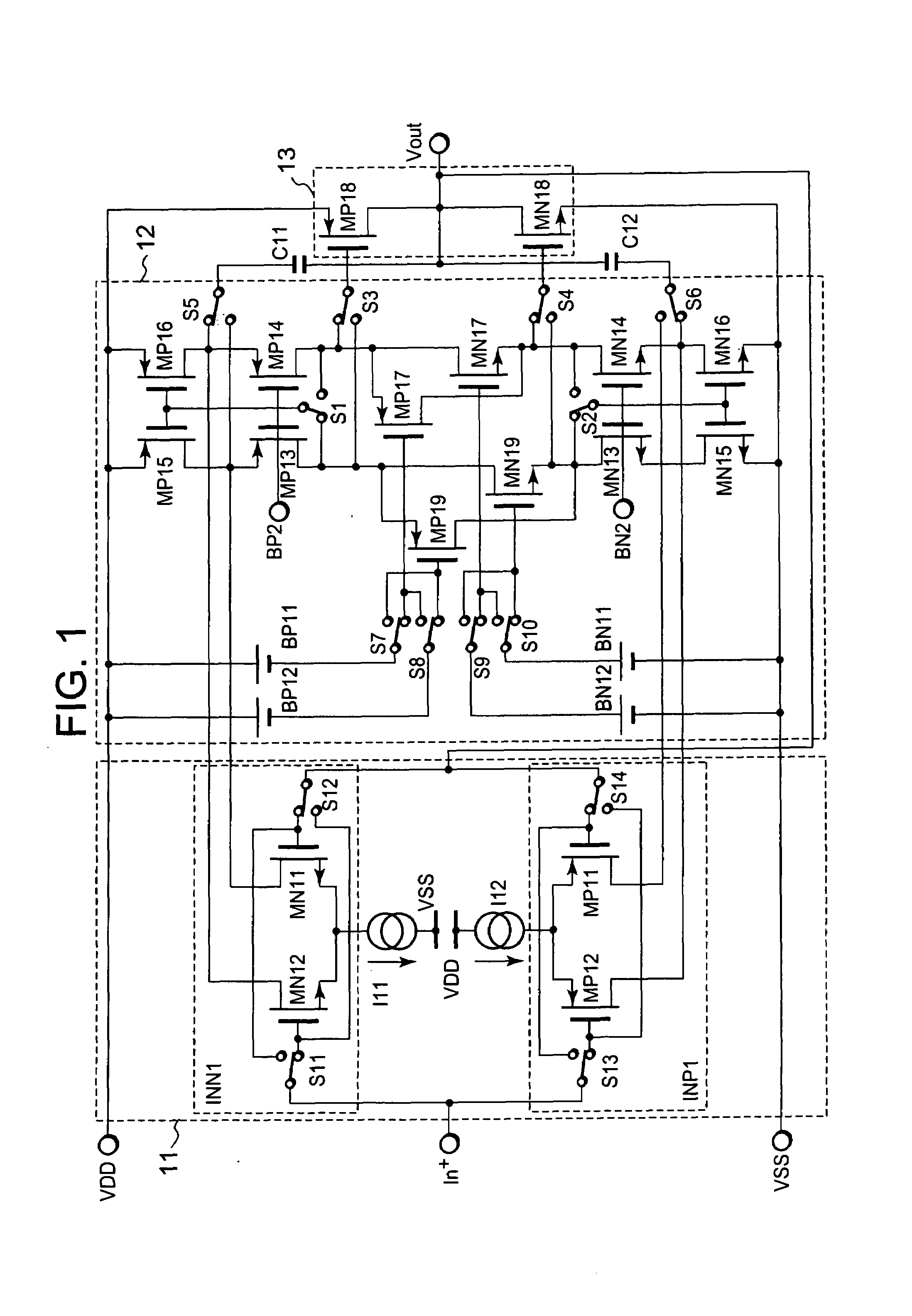
embodiment 2
[0063]FIG. 2 is a circuit diagram illustrating an operational amplifier of a second embodiment of the present invention. Like portions in FIG. 2 to the portions described in FIG. 1 are designated by like symbols and their description will be omitted. The circuit diagram shown in FIG. 2 illustrates an example in which a switch is eliminated from the circuit shown in FIG. 1.
[0064]Referring to FIG. 2, a node at which a source of a P channel MOS transistor MP27 and a drain of an N channel MOS transistor MN27 are commonly connected to each other is disconnected from the drain of the P channel MOS transistor MP14 shown in FIG. 1 and connected to a common terminal of a switch S3. Further, a node at which a drain of the P channel MOS transistor MP27 and a source of the N channel MOS transistor MN27 are commonly connected to each other is disconnected from the drain of the N channel MOS transistor MN14 shown in FIG. 1 and connected to a common terminal of a switch S4. Due to this connection,...
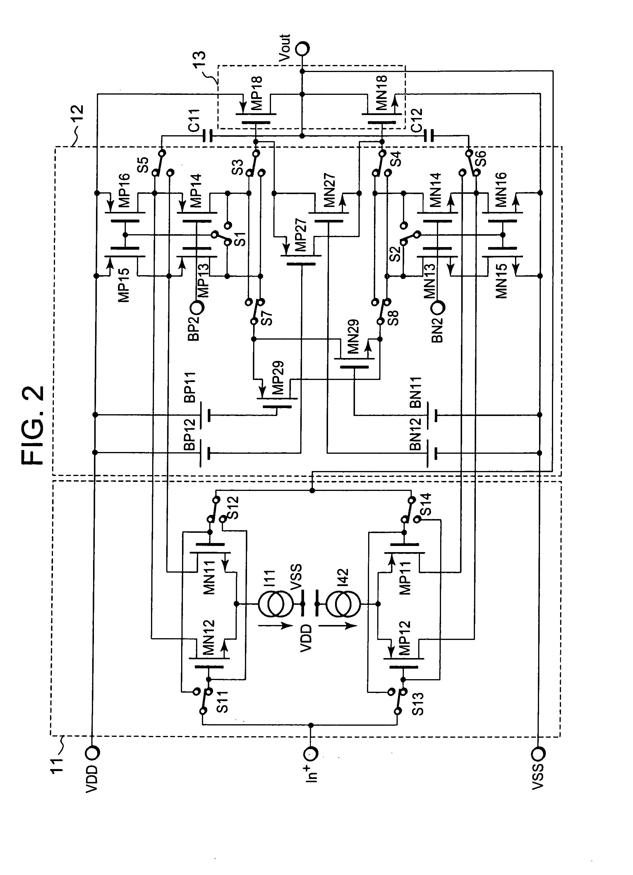
embodiment 3
[0068]FIG. 3 is a circuit diagram illustrating an operational amplifier of a third embodiment of the present invention. In the third embodiment, the P channel MOS transistor MP29 and the N channel MOS transistor MN29 supplying the floating current in the intermediate stage in FIG. 2 are changed in connection to configure a floating current source of another type.
[0069]Referring to FIG. 3, the floating current source in the present embodiment includes: N channel MOS transistors MN39, MN310 whose gates are commonly connected to each other; P channel MOS transistors MP39, MP310 whose gates are commonly connected to each other; a constant voltage source BN11 whose positive side is commonly connected to the gate and a drain of the P channel MOS transistor MP310 and whose negative side is connected to a GND potential; and a constant current source 133 one end of which is connected to a positive power terminal VDD and the other end of which is commonly connected to the gate and a drain of ...
PUM
 Abstract
Description
Claims
Application Information
 - R&D
- Intellectual Property
- Life Sciences
- Materials
- Tech Scout
- Unparalleled Data Quality
- Higher Quality Content
- 60% Fewer Hallucinations
Browse by: Latest US Patents, China's latest patents, Technical Efficacy Thesaurus, Application Domain, Technology Topic, Popular Technical Reports.
© 2025 PatSnap. All rights reserved.Legal|Privacy policy|Modern Slavery Act Transparency Statement|Sitemap|About US| Contact US: help@patsnap.com