Methods of forming vertical field effect transistors with self-aligned contacts and the resulting structures

a vertical field effect transistor and self-aligning technology, applied in the field of vertical field effect transistors, can solve the problems avoiding defects etc., to achieve the effect of forming gate contacts to such gates, and avoiding defects

Active Publication Date: 2019-10-29
GLOBALFOUNDRIES US INC
View PDF13 Cites 17 Cited by
  • Summary
  • Abstract
  • Description
  • Claims
  • Application Information

AI Technical Summary

Benefits of technology

[0008]Also disclosed herein are embodiments of a semiconductor structure formed according to the above-describe method embodiments. The semiconductor structure can include a vertical field effect transistor (VFET) on a substrate. This VFET can have a first end, a second end opposite the first end, and opposing sides and can include, but is not limited to, the following: a semiconductor fin that extends vertically between a lower source/drain region in the substrate and an upper source/drain region; a cap layer on the upper source/drain region; a spacer layer on the lower source/drain region and laterally surrounding the semiconductor fin; a gate on the spacer layer and later

Problems solved by technology

As the device density (i.e., the number of devices per unit area) of IC designs continues to be increased, forming vertical field effect transistors (VFETs) without violating design rules and/or risking the formation of defects (e.g., gate contact-to-upper source/drain region shorts, lower source/drain contact-to-gate shorts, etc.) can be difficult.
Howe

Method used


Image

  • Methods of forming vertical field effect transistors with self-aligned contacts and the resulting structures
  • Methods of forming vertical field effect transistors with self-aligned contacts and the resulting structures
  • Methods of forming vertical field effect transistors with self-aligned contacts and the resulting structures

Examples


Embodiment Construction

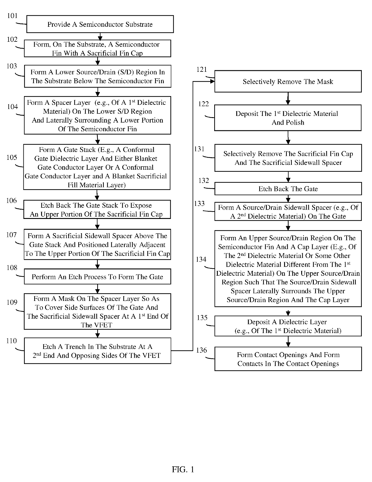
[0037]As mentioned above, as device density (i.e., the number of devices per unit area) of integrated circuit (IC) designs continues to be increased, forming vertical field effect transistors (VFETs) without violating design rules and / or risking the formation of defects (e.g., gate contact-to-upper source / drain region shorts, lower source / drain contact-to-gate shorts, etc.) can be difficult. For example, recently IC designs have been developed with a reduced fin pitch of 36 nm or less in order to increase device density in an array of VFETs. This reduction in fin pitch necessarily requires a corresponding reduction in the gate pitch to minimize parasitic capacitance. One recently developed technique for reducing gate pitch is the formation of a self-aligned gate (i.e., a gate where the shape of the gate is define during an etch process that uses a sidewall spacer formed on the gate stack as a mask). However, forming a gate contact to such a gate is problematic and typically requires...


PUM


Abstract

Disclosed are methods wherein vertical field effect transistor(s) (VFET(s)) and isolation region(s) are formed on a substrate. Each VFET includes a fin extending vertically between source/drain regions, a spacer layer and a gate around the fin, and a source/drain sidewall spacer around an upper source/drain region. Optionally, a gate sidewall spacer is adjacent to the gate at a first end of the VFET. An isolation region is adjacent to the gate at a second end and opposing sides of the VFET and extends into the substrate. Contacts are formed including a lower source/drain contact (which is adjacent to the first end of the VFET and is self-aligned if the optional gate sidewall spacer is present) and a self-aligned gate contact (which extends into the isolation region at the second end of the VFET and contacts a side surface of the gate). Also disclosed are structures formed according to the methods.

Description

BACKGROUNDField of the Invention[0001]The present invention relates to vertical field effect transistors (VFETs) and, more particularly, to methods of forming VFETs with self-aligned contacts and the resulting structures.Description of Related Art[0002]Integrated circuit (IC) design decisions are often driven by device scalability, device density, manufacturing efficiency and costs. As the device density (i.e., the number of devices per unit area) of IC designs continues to be increased, forming vertical field effect transistors (VFETs) without violating design rules and / or risking the formation of defects (e.g., gate contact-to-upper source / drain region shorts, lower source / drain contact-to-gate shorts, etc.) can be difficult. For example, recently IC designs have been developed with a reduced fin pitch of 36 nm or less in order to increase device density in an array of VFETs. This reduction in fin pitch necessarily requires a corresponding reduction in the gate pitch to minimize p...

Claims


Application Information

Patent Timeline
IPC IPC(8): H01L29/78H01L29/66H01L21/762H01L29/06
CPCH01L29/66575H01L21/762H01L29/0649H01L29/66666H01L29/7827H01L21/823885H01L21/823878H01L27/092H01L21/823871H01L21/76897
Inventor ZHANG, JOHN H.XIE, RUILONGKUMAR, MAHENDER
Owner GLOBALFOUNDRIES US INC
Why Eureka
Try Eureka