Flexible printed circuit

a printed circuit and flexible technology, applied in the association of printed circuit non-printed electric components, conductive material electric discharge removal, instruments, etc., can solve the problems of affecting the operation of portions, carbon coated polyester or paper was too expensive, and production rolls were not wide enough to achieve the effect of convenient folding

Active Publication Date: 2019-10-29
TF MASSIF TECH LTD
View PDF8 Cites 0 Cited by
  • Summary
  • Abstract
  • Description
  • Claims
  • Application Information

AI Technical Summary

Benefits of technology

[0004]There are a number of unique aspects to the flexible printed circuit described above. One aspect is the flexibility. The flexible supporting substrate with flexible conductive circuit has a planar operative position and has a stored position in a roll configuration, such that the flexible supporting substrate with conductive circuit can be rolled and unrolled at will to move between the operative position and the stored position. Alternatively, the flexible supporting substrate with conductive circuit can have a planar operative position and a stored position in a folded configuration, such that such that the flexible supporting substrate with conductive circuit can be folded and unfolded at will to move between the operative position and the stored position.

Problems solved by technology

Also of concern is how frequently the flexible supporting substrate may be rolled and unrolled, before there is a danger of material fatigue of the conductive material adversely affecting the operation of portions of the flexible conductive circuit.
Carbon coated polyester or paper was too expensive, production rolls were not wide enough and electrical resistance was too high.
Screen Printed silver conductive paste onto polyester was too expensive and required a screen or masking step as well as curing step.
With flexo-printed conductive silver paste onto polyester, resistance of conductive trace was too high, the rolls were not large enough and a curing step was needed.
Ink jet printed conductive material was too expensive and very few conductive jet-able inks are commercially available.
In addition, a curing step was need and the cost of equipment was prohibitive.
Should the sparking electrode become contaminated with burn-off, it will started to produce uneven lines and open breaks in the conductive pathways.
Ultrasonic ablation did not work, as it was slow and problematic.
Laser ablation crated too much heat and would burn through the supporting layer.
CNC Micro sandblasting was hard to control, produced uneven lines and left particulate matter that would need to be washed off Mask sandblasting required 2 masks, one for X direction and one for the Y direction.
It also would leave particulate needing to be washed off.
Direct soldering even under very controlled conditions was not successful due to heat damage to the material.
Ultrasonic and laser were not practical and the cost of a large area machine was prohibitive.
It did work to a limited extent but was prohibitive slow and fragile.
It was particularly prone to failure during roll up testing.
Direct attachment using film conductive adhesives was not practical as the footprint or attachment area of the LED's is too small to allow good bonding.
It was also prone to failure during Roll up testing.
Direct soldering even under very controlled conditions was not successful as heat damage to the material.
Conductive epoxy did not work as the epoxy was brittle and puller away from the flexible circuit during roll up testing.
Conventional connectors would not work because pitch or spacing of contact tabs is not conventional spacing due to limitations of material, electrical resistance and physical properties of the support material.
This was very time consuming with a possibility of mismatching connections.
A ridge circuit board with wires soldered to etched contact tabs was not reliable as one could not make consistent contact and needed some external clamping device to hold together.

Method used


Image

  • Flexible printed circuit
  • Flexible printed circuit
  • Flexible printed circuit

Examples


Embodiment Construction

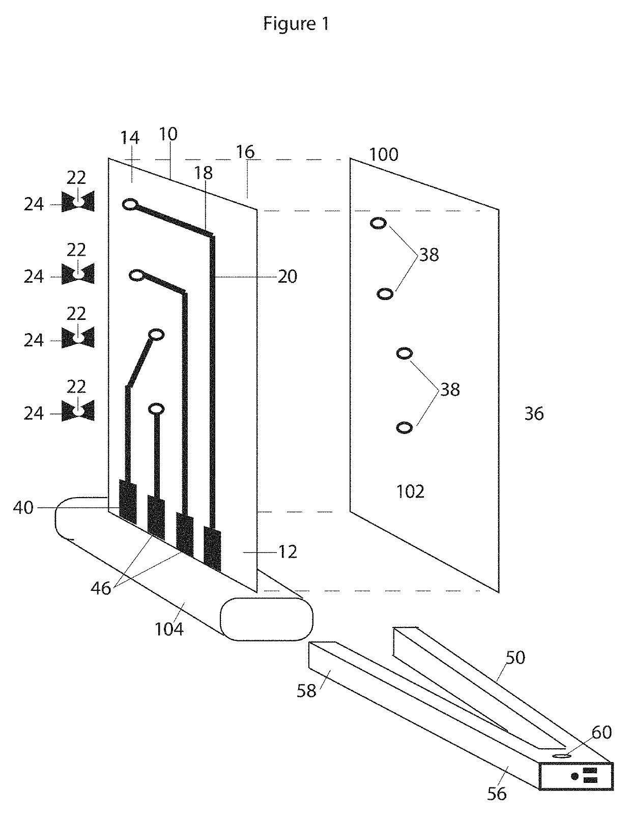
[0056]A flexible printed circuit generally identified by reference numeral 10, will now be described with reference to FIG. 1 through 28.

Structure and Relationship of Parts:

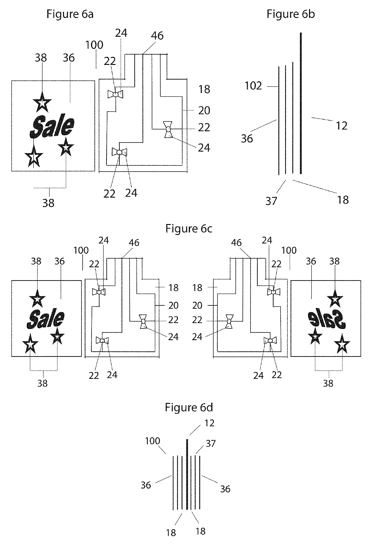
[0057]Referring to FIG. 1, there is illustrated a preferred embodiment of flexible printed circuit 10 which includes a flexible supporting substrate 12 having a first face 14 and a second face 16. Flexible printed circuit 10 is shown being used for a Point of Purchase (POP) display, generally indicated by reference numeral 100. In this preferred embodiment, flexible supporting substrate 12 is a polyester film. It will be appreciated that a plastic woven material or open pattern plastic material could be used. Conductive material 18 is positioned on first face 14, second face 16 or both first face 14 and second face 16. In this preferred embodiment, conductive material 18 is a conductive metal, preferably copper. A polyester film for supporting substrate 12 is preferred because a polyester film can be treated with...


PUM

PropertyMeasurementUnit
thicknessaaaaaaaaaa
thicknessaaaaaaaaaa
sizeaaaaaaaaaa

Abstract

A flexible printed circuit is described that includes a flexible supporting substrate having a first face and a second face. A conductive material is deposited by vacuum deposition on at least one of the first face or the second face of the flexible supporting substrate. A flexible conductive circuit is formed on the conductive material by electrical discharge machining. The flexible conductive circuit defines a plurality of electrical component placement circuits to which electrical components may be attached. The flexible printed circuit can be rolled or folded. The flexible printed circuit can also be made in sizes much larger than is currently possible with other competing technologies.

Description

FIELD[0001]There is described a flexible printed circuit that was developed for a point of purchase display stand. It is now realized that this flexible printed circuit has application beyond point of purchase display stands due to some unique properties that will hereinafter be further described.BACKGROUND[0002]Point of Purchase (POP) electrical stand-up displays are typically constructed by cutting a small hole out through rigid cardboard that has been imprinted with graphics. An LED is then manually pushed through the hole, so the LED protrudes from a front of the cardboard and is secured in place with tape positioned at a back of the cardboard. A conductive wire extends to a power transformer box, which is attached to the back of the cardboard by double sided adhesive tape. A power cord is run from the power transformer box to an external power outlet in a wall. When activated, the LED blinks on and off.SUMMARY[0003]There is provided a flexible printed circuit that includes a fl...

Claims


Application Information

Patent Timeline
Patent Type & Authority Patents(United States)
IPC IPC(8): H05K1/18H05K1/11H05K3/46G02F1/167G02F1/16755
CPCH05K1/118H05K1/189H05K2201/051H05K2201/10128H05K3/4685H05K2201/053G02F1/167H05K3/08H05K2201/055H05K2201/10106G02F1/16755H05K1/141H05K3/146A47F3/001A47F5/112
Inventor CAREL, ALAIN
Owner TF MASSIF TECH LTD
Why Eureka
Try Eureka