Method for forming regular polymer thin films using atmospheric plasma deposition

a technology of atmospheric plasma deposition and polymer thin film, which is applied in the direction of pretreatment surfaces, electric discharge tubes, coatings, etc., can solve the problems of preventing the application of cvd processes in many cases, affecting the practical application of cvd processes, and complex structure plasma-polymers obtained by cvd are ill suited for applications, etc., to achieve the effect of reducing the amount of energy, fast rise time and convenient adsorption

Active Publication Date: 2019-11-12
LUXEMBOURG INST OF SCI & TECH LIST
View PDF9 Cites 0 Cited by
  • Summary
  • Abstract
  • Description
  • Claims
  • Application Information

AI Technical Summary

Benefits of technology

[0029]The invention provides a method for forming functional and so-called smart polymer thin films, which require regular and linear polymer structures. By using methods in accordance with the present invention, conventional linear polymer or copolymer thin films may be grown by chain growth polymerization, by free radical polymerization, by controlled free radical polymerization, by step growth polymerization, by controlled oxidative polymerization and by ring opening polymerization. The process is operable at atmospheric pressure or pressures close to atmospheric pressure, which alleviates the need for equipment having sealed and pressure regulated deposition enclosures. This also allows the use of the process on substrates having complex geometries, as known processing enclosures are easily adapted for use with the process according to the invention. The method according to the invention does not necessarily require initiating agents or oxidants as it is the case in known CVD processes. The invention relies on very short current discharges, which may for example be induced by voltage pulses with fast rise time. It therefore uses less energy than known AP-DBD methods which use AC sinusoidal pulsed plasma at much higher duty-cycles. Less energy is therefore absorbed by the substrate, the temperature of which is not significantly altered by the impact of the pulsed plasma discharges. This in turn allows controlling the temperature of the substrate during deposition. For example, the substrate may be heated, which promotes the desorption of shorter polymer chains and smaller oligomers. Alternatively, the substrate may be cooled during deposition, thereby promoting the condensation of the monomer on the substrate's surface, which enhances the deposition rate. Due to the fast voltage rise time, short square pulsed AP-DBD in accordance with the invention is operating with distinct discharge current pulses at the voltage rising and falling phases. The produced short current discharge, with a large proportion of high energy electrons, efficiently induces the formation of free radicals that initiate the free radicals polymerization process. The short current discharge duration allows the use of duty-cycles far below 0.1%, while keeping tOFF in the millisecond range. The impact of the plasma discharge on the resulting thin film chemistry is thus minimized. On the other hand, the free radical polymerization reaction, occurring during more than 99.9% of the deposition process, is massively favored. Therefore, thin films composed of well-defined and defect-free polymer repeat units are grown using the invention.

Problems solved by technology

While such known processes generally generate good results, the conditions under which such processes are operated typically require a sealed and pressurized enclosure in the coating device.
This is a drawback as it requires expensive and technically involved coating devices, which impede the practical applications of CVD processes in many cases.
The complex structured plasma-polymers obtained by PE-CVD are ill suited for applications involving so-called smart functional layers, which allow for example to sense gas, which may be optically active or temperature sensitive, or which may be electrically conductive.
According to the prior art, regular polymer layer deposition has not been achieved using AP-DBD processes.
Such known processes are therefore hard to control, especially for obtaining the regular structures required in functional polymer thins films.

Method used


Image

  • Method for forming regular polymer thin films using atmospheric plasma deposition
  • Method for forming regular polymer thin films using atmospheric plasma deposition
  • Method for forming regular polymer thin films using atmospheric plasma deposition

Examples


Embodiment Construction

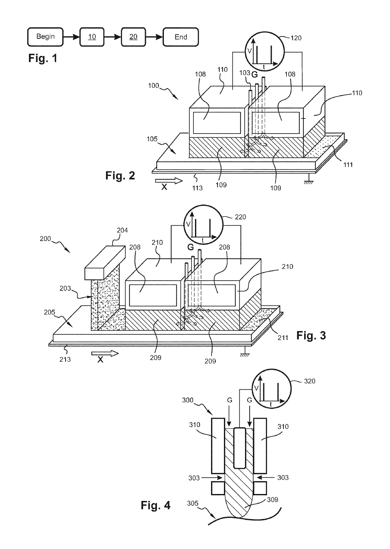
[0055]FIG. 1 is a flow chart, which illustrates the main steps of a preferred embodiment of the invention. In a first step 10, a mixture comprising at least one polymer forming material is provided. While the mixture may consist in only the polymer forming material as such, it may alternatively comprise other components, such as for example an organic solvent. The inclusion of such additional components may for example have an impact on the film deposition rate or on the porosity of the deposited layer. The polymer forming material is advantageously a monomer, which is chosen so that the regular and linear polymer chain comprising the monomer exhibits the properties, which the targeted application requires. Among the virtually infinite list of monomers that can be deposited by the method described herein, can be cited: N-isopropylacrylamide (NIPAAm), suitable for the growth of temperature responsive polymers; heptadecafluorodecylmethacrylate (HFDMA), suitable for the preparation of ...


PUM

PropertyMeasurementUnit
temperatureaaaaaaaaaa

Abstract

The invention provides a method for forming regular polymer thin films on a substrate using atmospheric plasma discharges. In particular, the method allows for the deposition of functional polymer thin films which require a high regularity and a linear polymer structure.

Description

FIELD OF THE INVENTION[0001]The present invention lies in the field of forming polymer thin films. In particular, the invention relates to forming thin films of regular polymers using plasma deposition techniques.BACKGROUND[0002]Polymers are long chains of organic molecules, which are assembled from many small repeating units, the monomers. The properties of polymers are very varied and can be tuned for specific applications by properly selecting the monomer identities, as well as their configuration and microstructure.[0003]It is known to use chemical vapor deposition, CVD, methods to form an organic coating on a substrate. CVD techniques allow for forming conformal thin films on a variety of substrate materials having a variety of geometries. The deposited films are substantially free of impurities such as solvents, initiators or plasticizers used in wet chemistry. CVD of organic coatings is usually accomplished by thermal or plasma activated processes. It is further known that va...

Claims


Application Information

Patent Timeline
Patent Type & Authority Patents(United States)
IPC IPC(8): B05D1/00H01J37/32B05D3/04
CPCH01J37/32192H01J37/32348B05D1/62B05D3/0486H01J2237/3321H01J37/3467
Inventor BOSCHER, NICOLASCHOQUET, PATRICKDUDAY, DAVIDHILT, FLORIAN
Owner LUXEMBOURG INST OF SCI & TECH LIST
Why Eureka
Try Eureka