Double gate, flexible thin-film transistor (TFT) complementary metal-oxide semiconductor (MOS) (CMOS) circuits and related fabrication methods

a technology of complementary metal-oxide semiconductors and thin-film transistors, which is applied in the direction of transistors, semiconductor devices, electrical equipment, etc., can solve the problems of small drive current and the inability to prevent high leakage current, so as to increase the maximum drive strength and channel on/off control, improve performance and power efficiency, and increase the maximum drive current

Active Publication Date: 2019-11-19
QUALCOMM INC
View PDF11 Cites 2 Cited by
  • Summary
  • Abstract
  • Description
  • Claims
  • Application Information

AI Technical Summary

Benefits of technology

[0004]Increasing the inversion channel layer in this regard can significantly increase the maximum drive strength and channel on / off control of the PFET and NFET in the TFT CMOS circuit. In this regard, employing double gate FETs can improve performance and power efficiency. Thus, a double gate, flexible TFT CMOS circuit fabricated according to methods disclosed herein is suited for applications requiring electronic circuits that can endure structural flexing, such as bending and folding in a wearable device or other conformable media, and also provide increased performance and / or battery life.

Problems solved by technology

The induced inversion channel may be so thin that the TFT device suffers from a high channel resistance, which leads to smaller drive current.
In addition, the channel on / off control provided by the gate may be too weak to prevent high leakage current.

Method used


Image

  • Double gate, flexible thin-film transistor (TFT) complementary metal-oxide semiconductor (MOS) (CMOS) circuits and related fabrication methods
  • Double gate, flexible thin-film transistor (TFT) complementary metal-oxide semiconductor (MOS) (CMOS) circuits and related fabrication methods
  • Double gate, flexible thin-film transistor (TFT) complementary metal-oxide semiconductor (MOS) (CMOS) circuits and related fabrication methods

Examples


Embodiment Construction

[0031]With reference now to the drawing figures, several exemplary aspects of the present disclosure are described. The word “exemplary” is used herein to mean “serving as an example, instance, or illustration.” Any aspect described herein as “exemplary” is not necessarily to be construed as preferred or advantageous over other aspects.

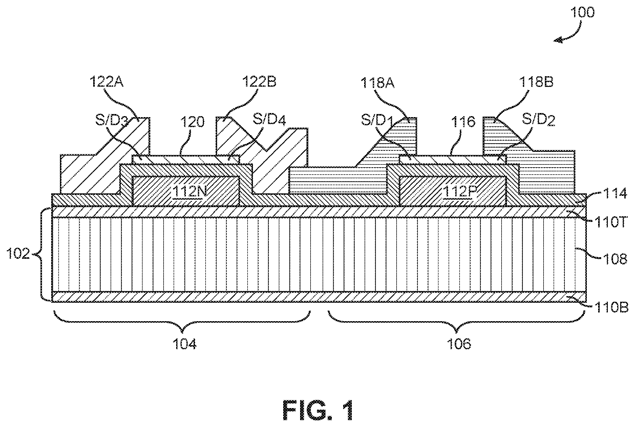
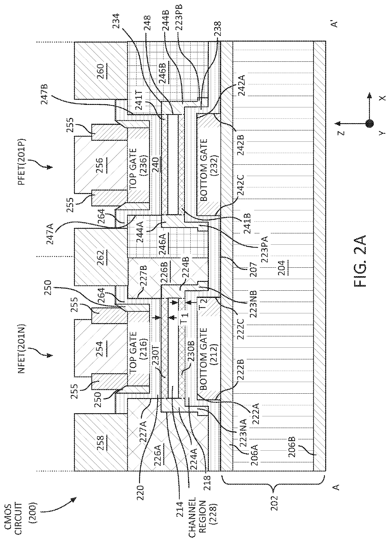
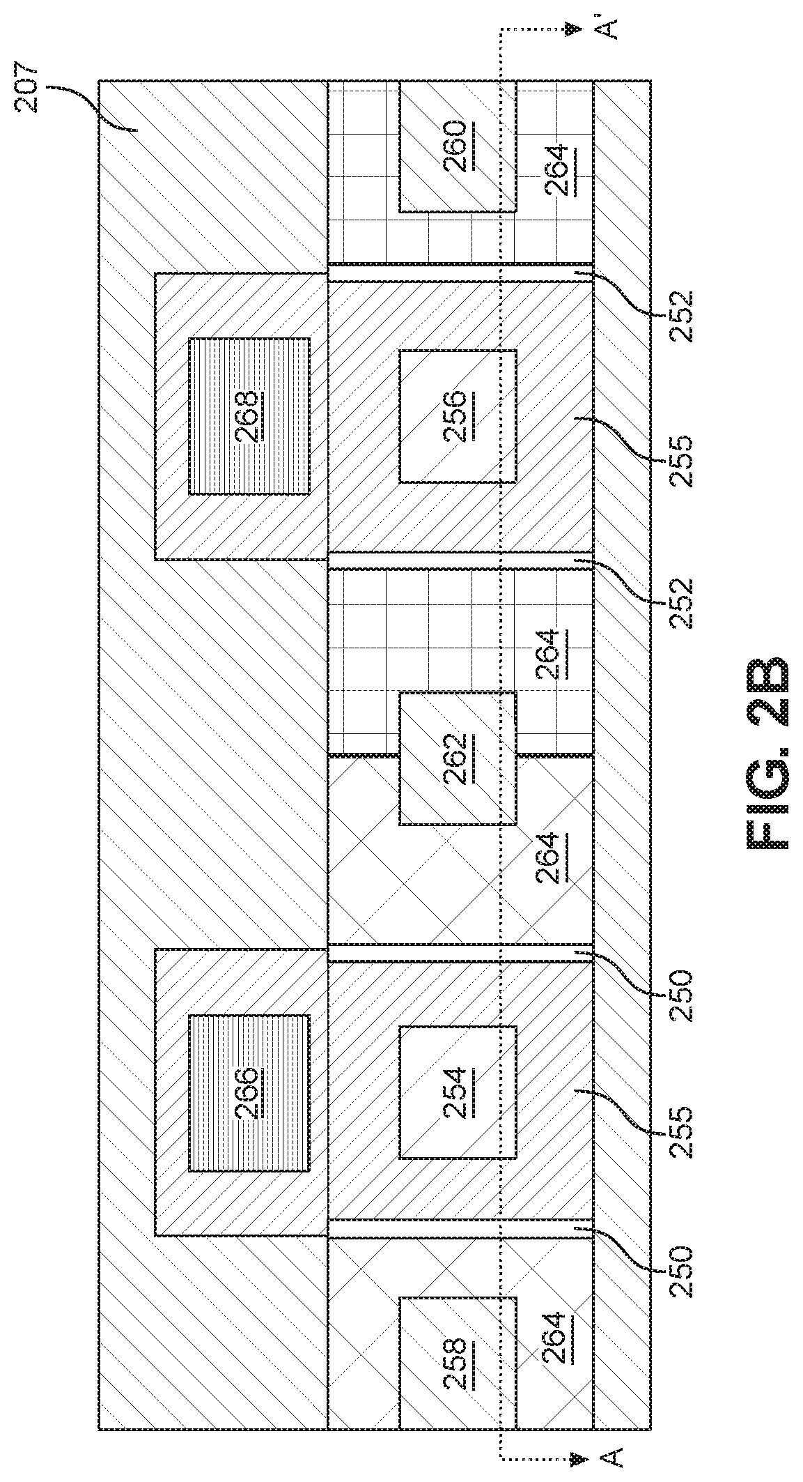
[0032]Aspects disclosed herein include double gate, flexible thin-film transistor (TFT) complementary metal-oxide semiconductor (MOS) (CMOS) circuits and related fabrication methods. For example, TFTs formed on flexible substrates are well suited to applications involving electronic devices incorporated into structurally flexible media, such as wearable devices, because the TFTs can withstand structural flexing that does not cause the electronic device to fail. In a flexible TFT CMOS circuit, a gate induces an inversion channel layer in a semiconductor material layer to provide a conduction channel. However, a thickness of the inversion channel layer ...


PUM


Abstract

Transistors formed on semiconductor substrates are not well-suited for integrated circuits employed in media designed to structurally flex to conform to a shaped surface or in response to physical stress. Structural flexing of wearable electronic devices, such as clothing, may cause cracking in the semiconductor substrate, resulting in failure of the integrated circuits. TFTs formed on flexible substrates can withstand structural flexing without failure. CMOS circuits are employed due to cost, performance, and power efficiency considerations. To provide increased drive strength for such applications, a flexible TFT structure for a CMOS circuit disclosed herein includes an exemplary NFET integrated with a complementary PFET on a flexible substrate. By forming a top gate on a semiconductor layer of a FET opposite to a bottom gate formed between the semiconductor layer and the flexible substrate, an effective thickness of an inversion channel layer induced in the semiconductor layer is doubled.

Description

BACKGROUNDI. Field of the Disclosure[0001]The technology of the disclosure relates generally to integrated circuits (ICs) formed on a flexible substrate and, more specifically, to complementary metal-oxide semiconductor (MOS) (CMOS) ICs employing thin film transistors (TFTs).II. Background[0002]A high level of functional capability is made possible in electronic devices by transistors, which are employed in large numbers in integrated circuits (ICs) within electronic devices. Central processing units (CPUs) and memory systems are examples of components in electronic devices that employ a large quantity of transistors in ICs. Such components are typically formed in or on rigid substrates in semiconductor wafers split into dies that are packaged as IC chips. The IC chips are mounted to a printed circuit board (PCB). For example, in a personal computer or hand-held mobile device, an IC chip that has a semiconductor die with a rigid substrate can be structurally supported and protected ...

Claims


Application Information

Patent Timeline
Patent Type & Authority Patents(United States)
IPC IPC(8): H01L27/12H01L29/786H01L29/10H01L21/8238H01L29/08
CPCH01L27/1262H01L29/0847H01L21/823864H01L29/78645H01L27/1225H01L29/7869H01L29/1033H01L27/1218H01L29/78648H01L29/78681
Inventor LI, XIAYANG, BINTAO, GENGMING
Owner QUALCOMM INC
Why Eureka
Try Eureka