Semiconductor element

a technology of semiconductor element and element, which is applied in the direction of transformer/inductance details, transformer/inductance coil/winding/connection, inductance, etc., can solve the problems of poor performance of quality factor and inductance value of the 8-shaped integrated, inductors and transformers, etc., to achieve different magnetic field coupling effects, flexible structure, and better symmetry

Active Publication Date: 2019-12-03
REALTEK SEMICON CORP
View PDF23 Cites 1 Cited by
  • Summary
  • Abstract
  • Description
  • Claims
  • Application Information

AI Technical Summary

Benefits of technology

[0004]In view of the issues of the prior art, an object of the present invention is to provide a semiconductor element to improve the performance and usability of integrated inductors and integrated transformers, so as to make an improvement to the prior art.
[0007]In the present invention, two spiral coils of a semiconductor element are connected by a connecting section. A relative position between the connecting section and the spiral coils varies in accordance with a practical use of the semiconductor element. In comparison with the prior art, the semiconductor element disposed in the present invention is better in symmetry and is more flexible in structure, such that the semiconductor element can be connected to application circuits in a more effective manner. Moreover, the semiconductor element disclosed in the present invention can achieve different magnetic field coupling effects by altering the ways the spiral coils are connected.

Problems solved by technology

However, inductors and transformers in integrated circuits often take up large areas; therefore, it becomes an important issue to reduce the areas of inductors and transformers in integrated circuits without degrading element performances, such as inductance, quality factor (Q), and coupling coefficient (K).
The 8-shaped integrated inductor 100 has an obvious drawback, that the spiral coil 110 or the spiral coil 120 itself has unsatisfactory symmetry, causing poor performances of the quality factor and the inductance value of the 8-shaped integrated inductor 100.

Method used


Image

  • Semiconductor element
  • Semiconductor element
  • Semiconductor element

Examples


Embodiment Construction

[0017]The following description is written by referring to terms of this technical field. If any term is defined in this specification, such term should be explained accordingly. In addition, the connection between objects or events in the below-described embodiments can be direct or indirect provided that these embodiments are practicable under such connection. Said “indirect” means that an intermediate object or a physical space exists between the objects, or an intermediate event or a time interval exists between the events.

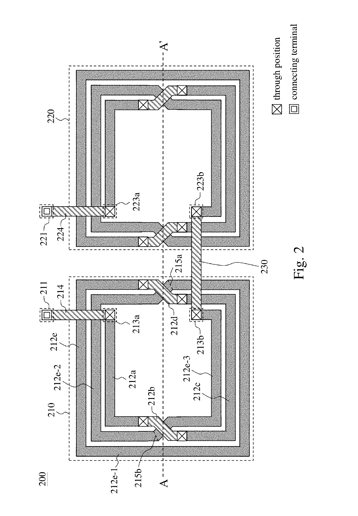
[0018]FIG. 2 shows a structure of a semiconductor element according to an embodiment of the present invention. The semiconductor element 200 includes two spiral coils 210 and 220. The spiral coils 210 and 220 are connected by a connecting section 230. As an example, the connecting section 230 can be formed by a metal segment. In this embodiment, the spiral coil 210 includes the metal segments 212a-212e. The metal segments 212b and 212d are fabricated in an upp...


PUM

PropertyMeasurementUnit
semiconductoraaaaaaaaaa
electric currentaaaaaaaaaa
symmetryaaaaaaaaaa

Abstract

A semiconductor element fabricated in a semiconductor structure and coupled to an application circuit through at least two connecting terminals. The semiconductor element includes a first spiral coil, a second spiral coil and a connecting portion. The first spiral coil is substantially located in a first metal layer and formed with a first end and a second end. The second spiral coil is substantially located in the first metal layer and formed with a third end and a fourth end. The connecting portion, which is located in a second metal layer, connects the second end and the fourth end. The first end is used as one of the two connecting terminals and the third end is used as the other of the two connecting terminals. The second metal layer is different from the first metal layer.

Description

BACKGROUND OF THE INVENTION1. Field of the Invention[0001]The present invention relates to semiconductor element, especially to an integrated inductor and an integrated transformer.2. Description of Related Art[0002]Inductors and transformers are important elements in radio frequency integrated circuits to implement single-ended to differential signal conversion, signal coupling and impedance matching. As System-on-chips (SoCs) become the mainstream of integrated circuits, integrated inductors and integrated transformers are gradually substituted for conventional discrete elements and are commonly applied to radio frequency integrated circuits. However, inductors and transformers in integrated circuits often take up large areas; therefore, it becomes an important issue to reduce the areas of inductors and transformers in integrated circuits without degrading element performances, such as inductance, quality factor (Q), and coupling coefficient (K).[0003]FIG. 1 illustrates a structur...

Claims


Application Information

Patent Timeline
Patent Type & Authority Patents(United States)
IPC IPC(8): H01F5/00H01L23/522H01F27/29H01F27/28H01L49/02
CPCH01L23/5227H01F27/2804H01F27/29H01L28/10H01F2027/2809H01F17/0006H01F2017/0046H01F2017/0073H01F2017/0086
Inventor YEN, HSIAO-TSUNGLUO, CHENG-WEIJEAN, YUH-SHENGYEH, TA-HSUN
Owner REALTEK SEMICON CORP
Why Eureka
Try Eureka