
Display device and operation method thereof, and electronic device

a technology of display device and operating method, which is applied in the direction of transistors, diodes, instruments, etc., can solve the problems of deteriorating display quality, users of display device might feel glare under weak external light, and display quality deterioration, so as to prolong the non-lighting time of backlight, prolong the lighting time of backlight, and ensure the effect of brightness

Active Publication Date: 2019-12-24
SEMICON ENERGY LAB CO LTD
View PDF30 Cites 1 Cited by
  • Summary
  • Abstract
  • Description
  • Claims
  • Application Information

AI Technical Summary

Benefits of technology

The present invention provides a display device and operating method that can display low-luminance images with high display quality, without causing unevenness or glare under external light. Additionally, the display device has low power consumption, is highly reliable, and operates at high speed. The invention also provides a novel display device and operating method.

Problems solved by technology

Therefore, when a dark image is to be displayed, unevenness in luminance, color, and the like are generated in the displayed image, resulting in deterioration of the display quality.
In order to keep display quality at a certain level or higher, it is necessary to display an image whose luminance is at a certain level or higher; however, users of the display device might feel glare under weak external light.
Therefore, as in the above display device including the backlight, unevenness in luminance, color, and the like are generated in the displayed image, resulting in deterioration of the display quality.

Method used


Image

  • Display device and operation method thereof, and electronic device
  • Display device and operation method thereof, and electronic device
  • Display device and operation method thereof, and electronic device

Examples


embodiment 1

(Embodiment 1)

[0082]In this embodiment, configuration examples of a display device of one embodiment of the present invention will be described with reference drawings.

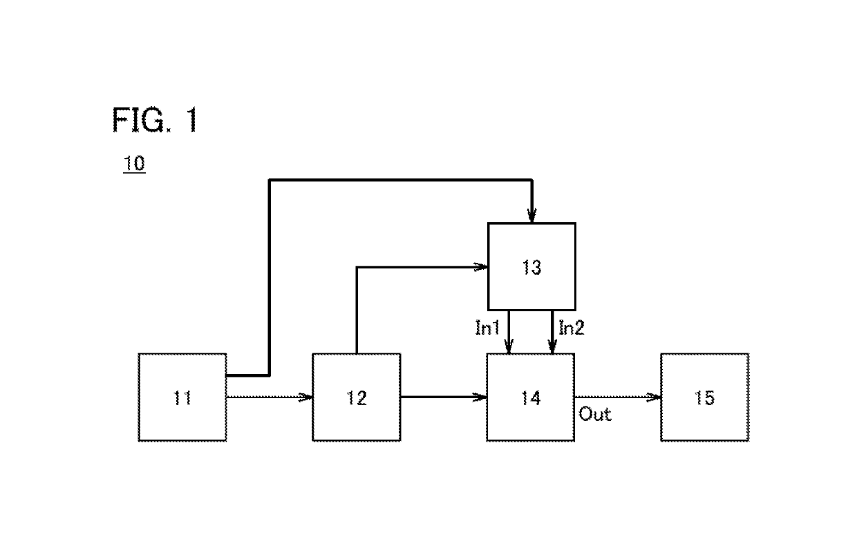
[0083]One embodiment of the present invention relates to a display device including an arithmetic circuit, a digital data converter circuit, an input signal generation circuit, a digital-to-analog (D / A) converter circuit, and a display portion and an operation method thereof. Note that the display portion includes a display element, and, for example, a light-emitting element such as an organic EL element can be used as the display element.

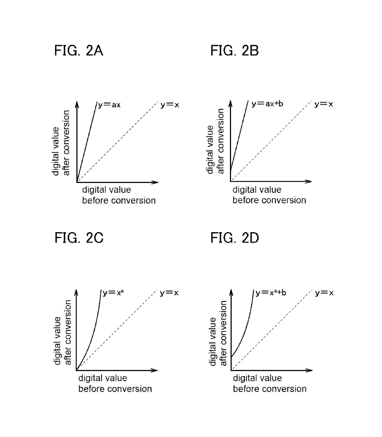
[0084]The arithmetic circuit has a function of generating digital display data, and the display data contains information on luminance of an image displayed on the display portion. For example, in the case where luminance of the image displayed on the display portion is represented by 8 bits, the luminance of the image displayed on the display portion is the lowest when the digital v...

embodiment 2

(Embodiment 2)

[0156]In this embodiment, a display device of one embodiment of the present invention and a manufacturing method thereof will be described.

[0157]The display device of one embodiment of the present invention has a structure in which a first display panel and a second display panel are bonded to each other with an adhesive layer therebetween. In the first display panel, first pixels that include reflective liquid crystal elements are provided. In the second display panel, second pixels that include light-emitting elements are provided. The reflective liquid crystal elements can produce gray levels by controlling the amount of reflected light. The light-emitting elements can produce gray levels by controlling the amount of light emission.

[0158]Note that the first pixel may include a transmissive liquid crystal element. In that case, the light-emitting element included in the second pixel can be used as a backlight. Note that in the case where a polarizing film is not prov...

example 1

[Structure Example 1]

[0188]FIG. 10 is a schematic cross-sectional view of the display device 10. In the display device 10, a display panel 100 and a display panel 200 are bonded to each other with an adhesive layer 50. The display device 10 includes a substrate 611 on the rear side (the side opposite to the viewing side) and a substrate 612 on the front side (the viewing side).

[0189]The display panel 100 includes a transistor 110 and a light-emitting element 120 between a resin layer 101 and a resin layer 102. The display panel 200 includes a transistor 210 and a liquid crystal element 220 between a resin layer 201 and a resin layer 202. The resin layer 101 is bonded to the substrate 611 with an adhesive layer 51 positioned therebetween. The resin layer 202 is bonded to the substrate 612 with an adhesive layer 52 positioned therebetween.

[0190]The resin layer 102, the resin layer 201, and the resin layer 202 are each provided with an opening. A region 81 illustrated in FIG. 10 is a r...


PUM

PropertyMeasurementUnit
voltageaaaaaaaaaa
voltageaaaaaaaaaa
voltageaaaaaaaaaa

Abstract

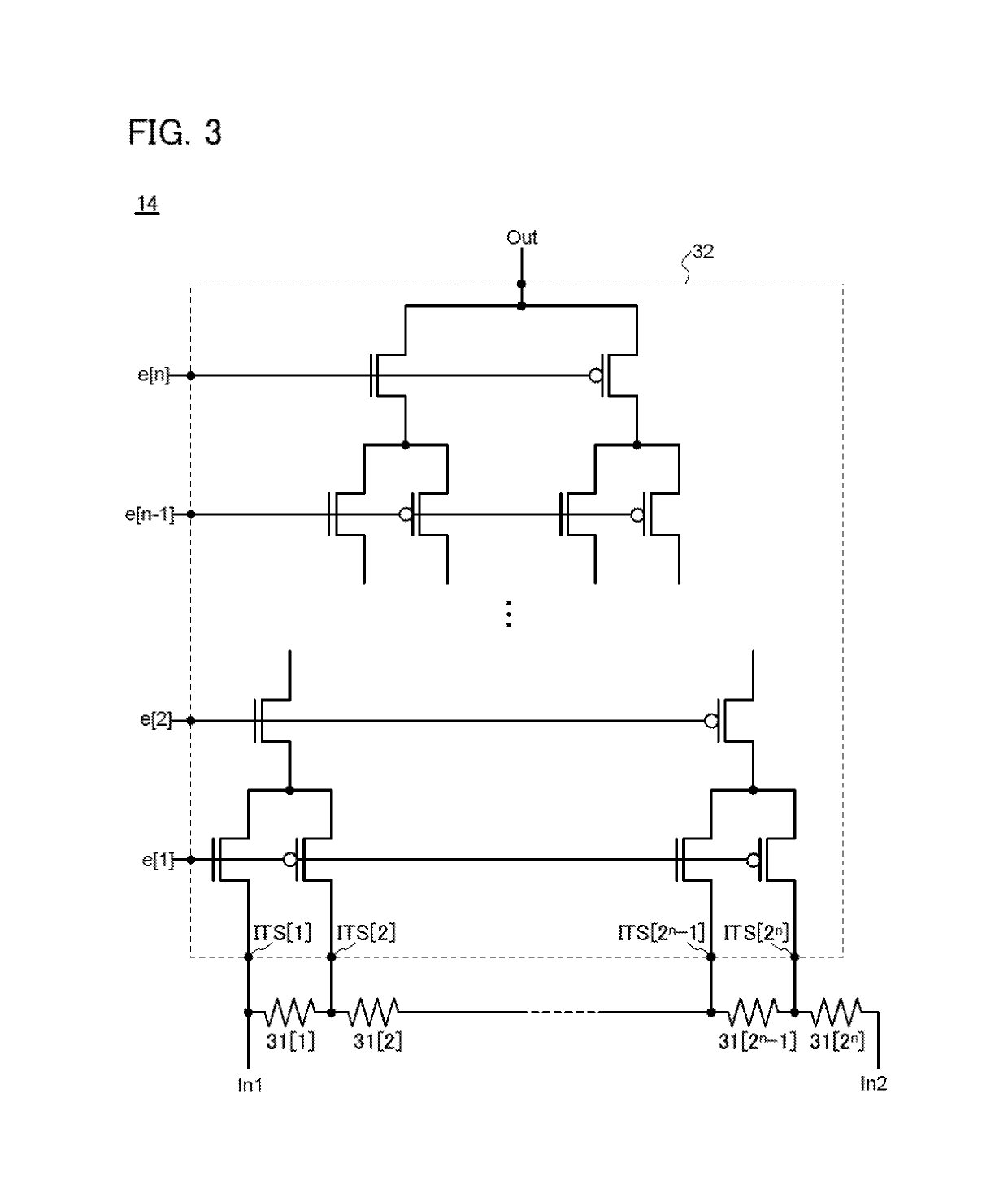
A first circuit generates first display data that is digital data which has information on luminance of an image displayed on a display portion. A second circuit generates second display data that is digital data obtained by converting a digital value of the first display data. A third circuit generates a first analog signal and a second analog signal whose potentials are calculated on the basis of the digital value of the first display data. The potential of the second analog signal is lower than the potential of the first analog signal. A fourth circuit converts the second display data into third display data that is analog data. A potential of the third display data is calculated on the basis of the potential of the first analog signal, the potential of the second analog signal, and a digital value of the second display data.

Description

BACKGROUND OF THE INVENTION[0001]1. Field of the Invention[0002]One embodiment of the present invention relates to a display device, an operating method thereof, and an electronic device.[0003]Note that one embodiment of the present invention is not limited to the above technical field. The technical field of one embodiment of the invention disclosed in this specification and the like relates to an object, a method, or a manufacturing method. Furthermore, one embodiment of the present invention relates to a process, a machine, manufacture, or a composition of matter. Specific examples of the technical field of one embodiment of the present invention disclosed in this specification and the like include a semiconductor device, a display device, a light-emitting device, a power storage device, a memory device, a method for driving any of them, and a method for manufacturing any of them.[0004]2. Description of the Related Art[0005]A liquid crystal display device in which a surface-emitt...

Claims


Application Information

Patent Timeline
Patent Type & Authority Patents(United States)
IPC IPC(8): G02F1/1335G09G5/10G09G3/34G09G3/36H01L27/32G09G3/20H01L27/12G09G3/3208G09G3/3225H01L29/786
CPCG09G3/3648G02F1/133603G09G3/3413G09G3/2003G09G3/3696H01L27/3232G09G3/3426G02F1/133553G09G5/10G09G3/36H01L2227/326G09G2310/027G09G3/3208H01L2227/323G09G2320/0233G09G2300/023G09G2360/144G02F2201/44G09G2330/021G09G2320/0242G09G3/3225H01L27/1225G09G2320/0238H01L29/7869H10K71/80H10K59/1201H10K59/50
Inventor IKEDA, TAKAYUKI
Owner SEMICON ENERGY LAB CO LTD
Learn More