Method and apparatus for reproducing component of semiconductor manufacturing apparatus, and reproduced component

a semiconductor manufacturing and component technology, applied in the direction of coatings, chemical vapor deposition coatings, electric discharge tubes, etc., can solve the problems of increasing the production cost of semiconductor products, the difficulty of smoothly performing the etching process, etc., and achieve the effect of reducing industrial waste and reducing the production cost of the final semiconductor produ

Active Publication Date: 2020-03-10
TOKAI CARBON CO LTD
View PDF26 Cites 0 Cited by
  • Summary
  • Abstract
  • Description
  • Claims
  • Application Information

AI Technical Summary

Benefits of technology

[0009]The present disclosure is to solve the foregoing problems, and an aspect of the present disclosure is to provide a method and apparatus for reproducing a component of a semiconductor manufacturing apparatus, and a reproduced component which may contribute to an environmental preservation by reducing industrial wastes caused by discarding consumable components, for example, replaceable focus rings, of the semiconductor manufacturing apparatus and may reduce production costs of a final semiconductor product.

Problems solved by technology

When the focus ring is not replaced at an appropriate time, it may be difficult to smoothly perform an etching process due to an increase in an amount of by-products created by etching the focus ring.
To precisely etch a wafer, the other components damaged due to etching may also need to be replaced by new components at preset intervals, which may lead to an increase in production costs of semiconductor products.

Method used


Image

  • Method and apparatus for reproducing component of semiconductor manufacturing apparatus, and reproduced component
  • Method and apparatus for reproducing component of semiconductor manufacturing apparatus, and reproduced component
  • Method and apparatus for reproducing component of semiconductor manufacturing apparatus, and reproduced component

Examples


Embodiment Construction

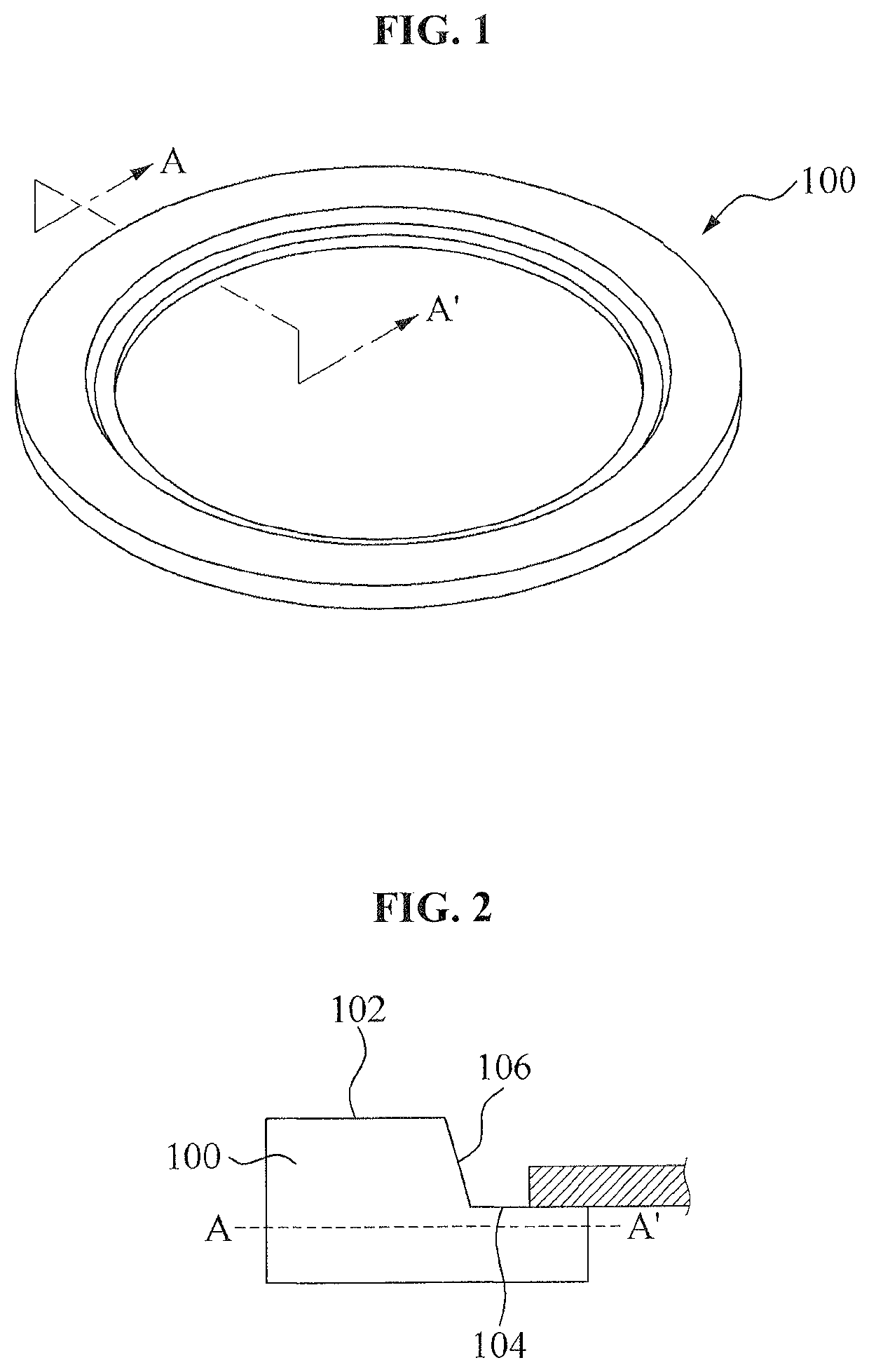
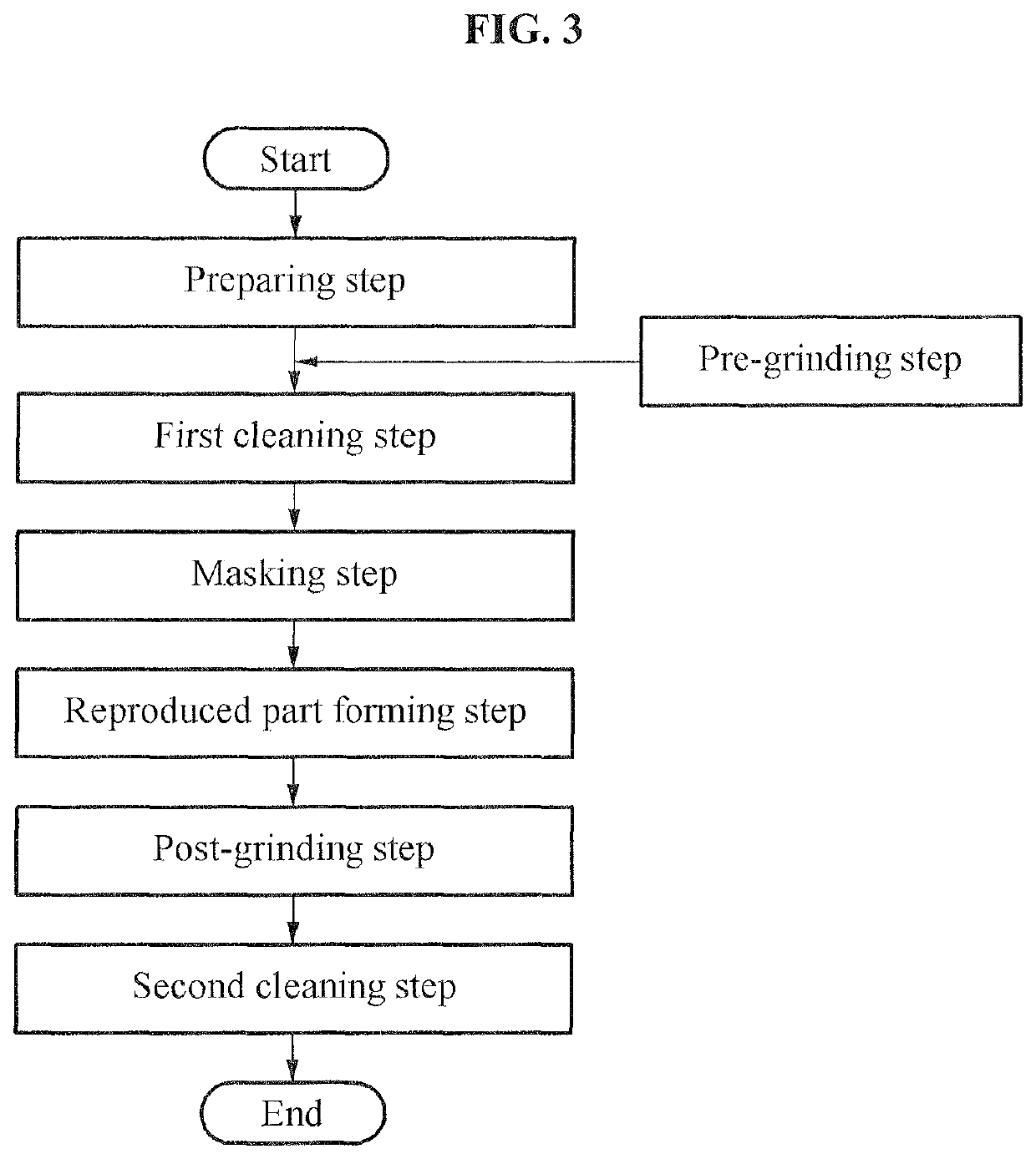
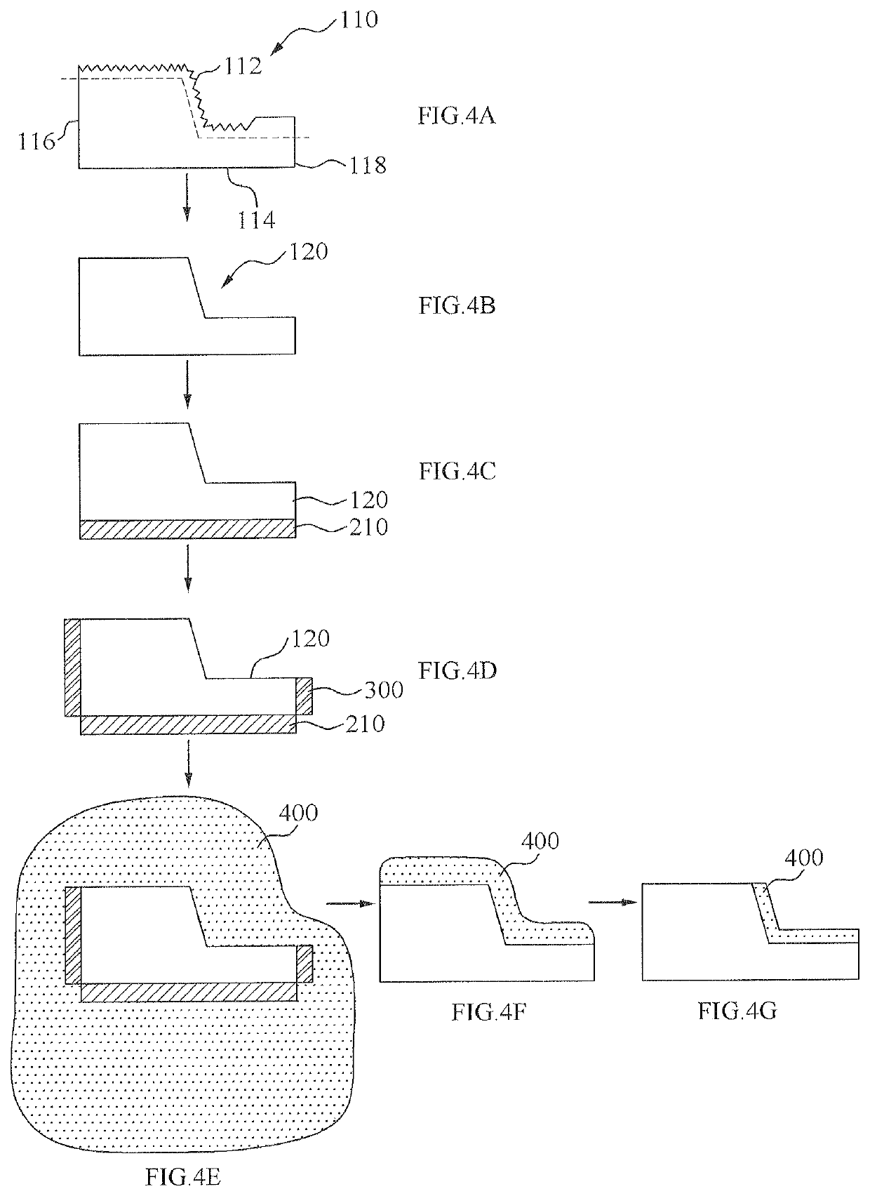
[0047]Hereinafter, a method and apparatus for reproducing a component of a semiconductor manufacturing apparatus, and a reproduced component will be described in detail with reference to example embodiments and drawings. Various alterations and modifications may be made to the example embodiments and drawings. When describing the example embodiments with reference to the accompanying drawings, like reference numerals refer to like elements, and a repeated description related thereto will be omitted. Here, the example embodiments are not construed as limited to the disclosure and should be understood to include all changes, equivalents, and replacements within the idea and the technical scope of the disclosure. When it is determined detailed description related to a related known function or configuration they may make the purpose of the present disclosure unnecessarily ambiguous in describing the present disclosure, the detailed description will be omitted here.

[0048]Also, terms use...


PUM

PropertyMeasurementUnit
thicknessaaaaaaaaaa
temperatureaaaaaaaaaa
deposition rateaaaaaaaaaa

Abstract

A method and apparatus for reproducing a component of a semiconductor manufacturing apparatus, and a reproduced component are provided. The method may include a preparing step of preparing a damaged component of a semiconductor manufacturing apparatus, a first cleaning step of cleaning the damaged component, a masking step of masking at least one of areas including an undamaged part of the damaged component, a reproduced part forming step of forming a reproduced part on the damaged component using a chemical vapor deposition (CVD), a post-grinding step of grinding the damaged component with the reproduced part, and a second cleaning step of cleaning the damaged component with the reproduced part.

Description

CROSS-REFERENCE TO RELATED APPLICATIONS[0001]This application claims the benefit of Korean Patent Application No. 10-2016-0064388 filed on May 25, 2016, in the Korean Intellectual Property Office, the disclosure of which is incorporated herein by reference.BACKGROUND[0002]1. Field of the Invention[0003]One or more example embodiments relate to a method and apparatus for reproducing a component of a semiconductor manufacturing apparatus, and a reproduced component, and more particularly, relate to a method and apparatus for reproducing a component of a semiconductor manufacturing apparatus which are available in a semiconductor manufacturing process by reproducing a damaged component of a dry etching apparatus using plasma, and relate to a reproduced component.[0004]2. Description of the Related Art[0005]Generally, a plasma etching scheme used in a semiconductor manufacturing process is one of dry etching processes and is performed to etch a target using gas. In the plasma etching sc...

Claims


Application Information

Patent Timeline
Patent Type & Authority Patents(United States)
IPC IPC(8): H01J37/32C23C16/02C23C16/56C23C16/04C23C16/44
CPCC23C16/4401C23C16/042C23C16/56C23C16/0227C23C16/0254H01J37/32009H01J37/32642H01J37/32532H01J37/3255H01J2237/334H01L21/02032H01L21/02052H01L21/02057H01L21/02079
Inventor KIM, KI WONROH, HYEONG UKYUN, JONG SUNGHONG, WON PYO
Owner TOKAI CARBON CO LTD
Why Eureka
Try Eureka