

Imaging lens assembly, image capturing unit and electronic device
a technology of image capturing unit and lens assembly, which is applied in the direction of lenses, optics, instruments, etc., can solve the problems of reducing the camera size, unfavorable installation of telephoto cameras in compact portable electronic devices, and low image brightness
- Summary
- Abstract
- Description
- Claims
- Application Information
AI Technical Summary
Benefits of technology
Problems solved by technology
Method used
Image

Examples
1st embodiment
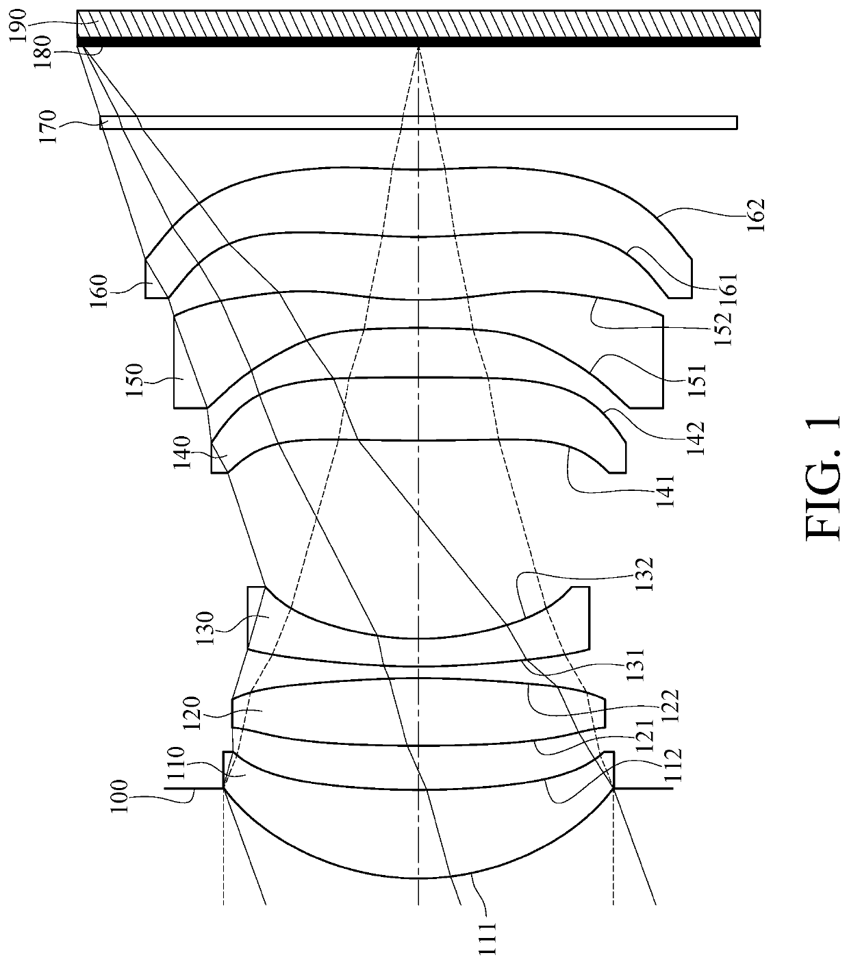
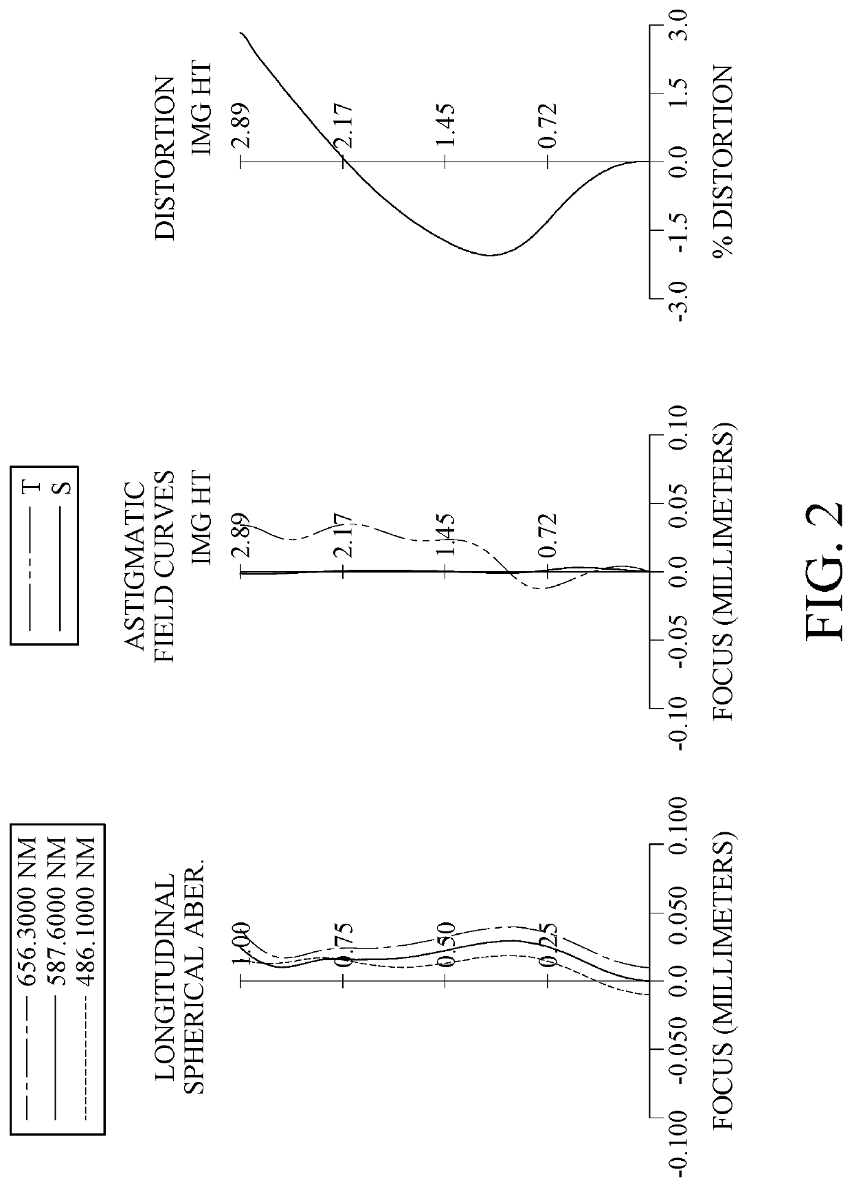
[0093]FIG. 1 is a schematic view of an image capturing unit according to the 1st embodiment of the present disclosure. FIG. 2 shows, in order from left to right, spherical aberration curves, astigmatic field curves and a distortion curve of the image capturing unit according to the 1st embodiment. In FIG. 1, the image capturing unit includes the imaging lens assembly (its reference numeral is omitted) of the present disclosure and an image sensor 190. The imaging lens assembly includes, in order from an object side to an image side, an aperture stop 100, a first lens element 110, a second lens element 120, a third lens element 130, a fourth lens element 140, a fifth lens element 150, a sixth lens element 160, a filter 170 and an image surface 180. The imaging lens assembly includes six single and non-cemented lens elements (110, 120, 130, 140, 150 and 160) with no additional lens element disposed between each of the adjacent six lens elements, wherein there is an air gap between eve...
2nd embodiment
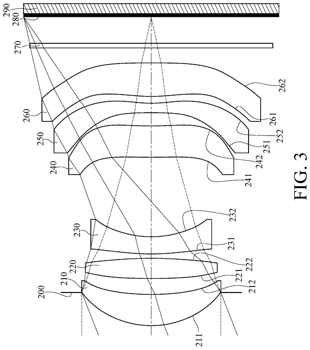
[0137]FIG. 3 is a schematic view of an image capturing unit according to the 2nd embodiment of the present disclosure. FIG. 4 shows, in order from left to right, spherical aberration curves, astigmatic field curves and a distortion curve of the image capturing unit according to the 2nd embodiment. In FIG. 3, the image capturing unit includes the imaging lens assembly (its reference numeral is omitted) of the present disclosure and an image sensor 290. The imaging lens assembly includes, in order from an object side to an image side, an aperture stop 200, a first lens element 210, a second lens element 220, a third lens element 230, a fourth lens element 240, a fifth lens element 250, a sixth lens element 260, a filter 270 and an image surface 280. The imaging lens assembly includes six single and non-cemented lens elements (210, 220, 230, 240, 250 and 260) with no additional lens element disposed between each of the adjacent six lens elements, wherein there is an air gap between eve...
3rd embodiment
[0152]FIG. 5 is a schematic view of an image capturing unit according to the 3rd embodiment of the present disclosure. FIG. 6 shows, in order from left to right, spherical aberration curves, astigmatic field curves and a distortion curve of the image capturing unit according to the 3rd embodiment. In FIG. 5, the image capturing unit includes the imaging lens assembly (its reference numeral is omitted) of the present disclosure and an image sensor 390. The imaging lens assembly includes, in order from an object side to an image side, a first lens element 310, an aperture stop 300, a second lens element 320, a third lens element 330, a fourth lens element 340, a fifth lens element 350, a sixth lens element 360, a filter 370 and an image surface 380. The imaging lens assembly includes six single and non-cemented lens elements (310, 320, 330, 340, 350 and 360) with no additional lens element disposed between each of the adjacent six lens elements, wherein there is an air gap between eve...
PUM
 Abstract
Description
Claims
Application Information