
Electronic product

a technology of electronic products and connecting holes, which is applied in the direction of electrical equipment, semiconductor devices, semiconductor/solid-state device details, etc., can solve the problems of reducing the life time of electronic products and the electronic product, and achieve the enhancement of the time that water vapor reaches the metal pattern through the connecting hole, the effect of enhancing the life time and reliability of electronic products

Active Publication Date: 2020-04-28
HANNSTAR DISPLAY CORPORATION
View PDF2 Cites 0 Cited by
  • Summary
  • Abstract
  • Description
  • Claims
  • Application Information

AI Technical Summary

Benefits of technology

[0004]The present invention provides an electronic product having a bonding pad structure, and a specific spacing exists between a connecting hole and an edge of the bonding pad structure, such that a water vapor damage of the bonding pad structure is mitigated, thereby enhancing the life time and reliability of the electronic product.
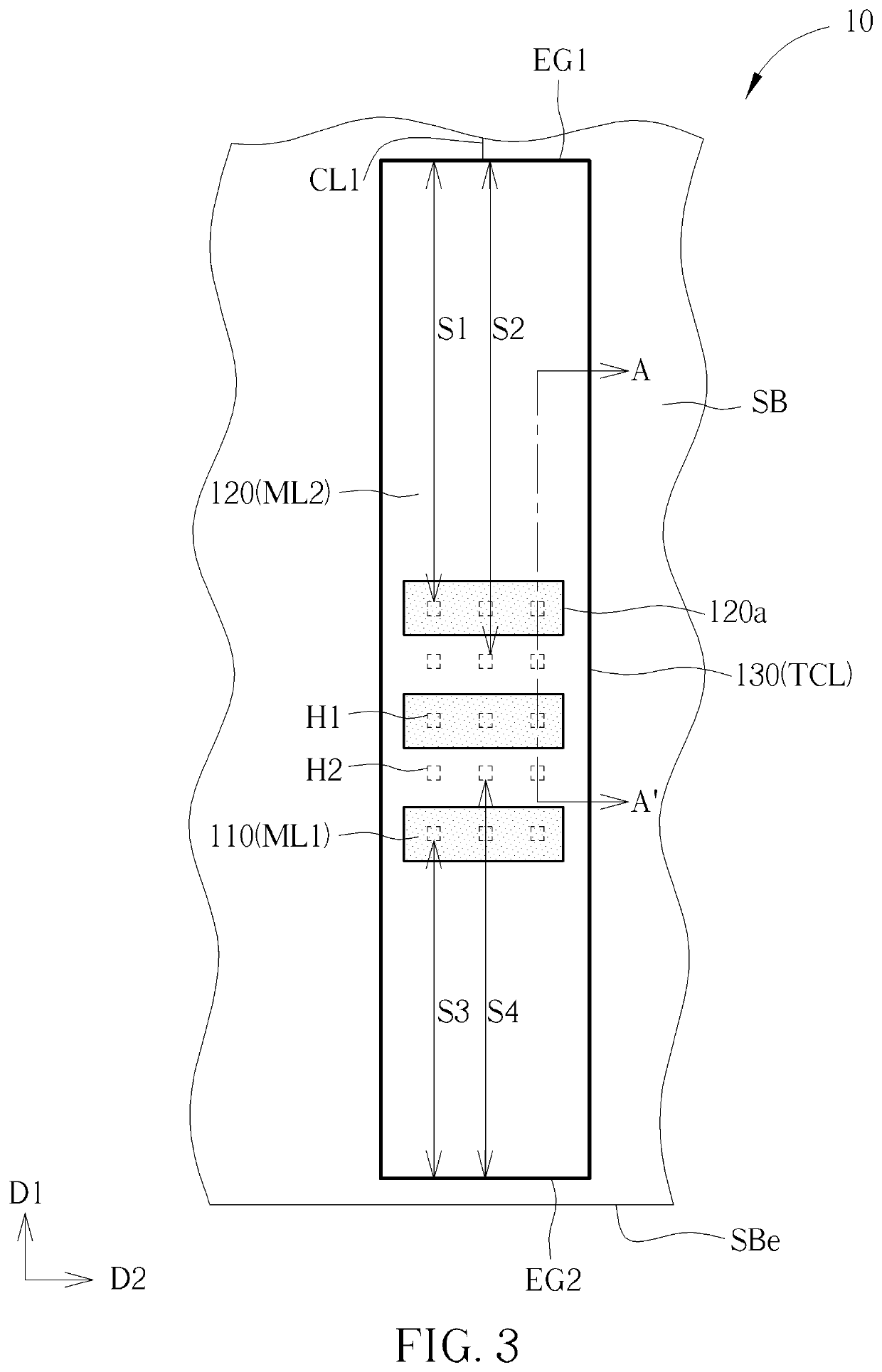
[0006]In the electronic product of the present invention, the connecting hole of the bonding pad structure is separated from the edge of the bonding pad structure by a specific distance; that is to say, the spacing between the connecting hole and the edge of the bonding pad structure is greater than or equal to 100 μm. Therefore, the path length that the water vapor invades the connecting hole is increased. As the result, the time that the water vapor reaches the metal pattern through the connecting hole is significantly enhanced, so as to retard the phenomenon of eroding the metal pattern, protect the bonding pad structure and enhance the life time and reliability of the electronic product.

Problems solved by technology

However, when the water vapor invade the conventional electronic product, the bonding pad of the electronic product is damaged by the water vapor easily, such that the conductive path is damaged to cause the breakdown of the electronic product and decrease the life time of the electronic product.

Method used


Image

  • Electronic product
  • Electronic product
  • Electronic product

Examples


Embodiment Construction

[0015]To provide a better understanding of the present invention to those skilled in the art, preferred embodiments will be detailed in the follow description. The preferred embodiments of the present invention are illustrated in the accompanying drawings with numbered elements to elaborate on the contents and effects to be achieved. It should be noted that the drawings are simplified schematics, and therefore show only the components and combinations associated with the present invention, so as to provide a clearer description for the basic structure or implementing method of the present invention. The components would be more complex in reality. In addition, for ease of explanation, the components shown in the drawings may not represent their actual number, shape, and dimensions; details may be adjusted according to design requirements.

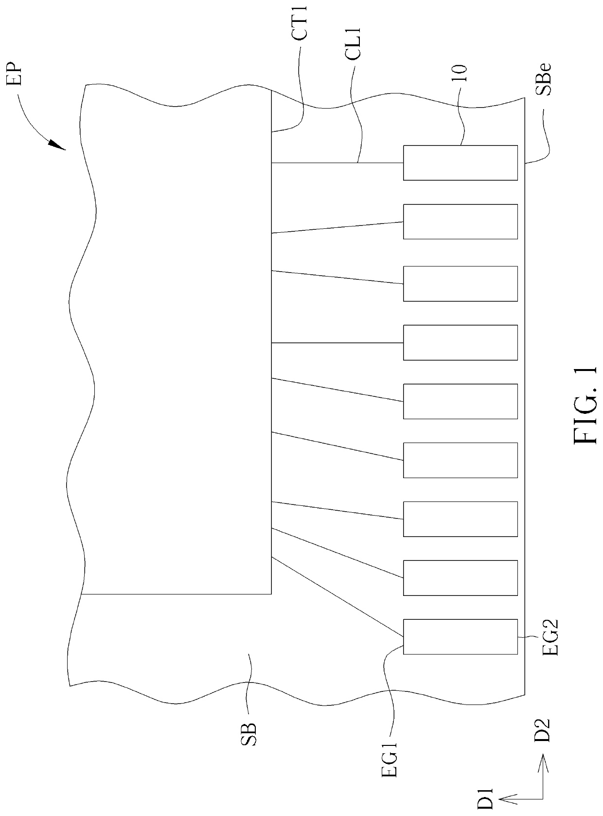
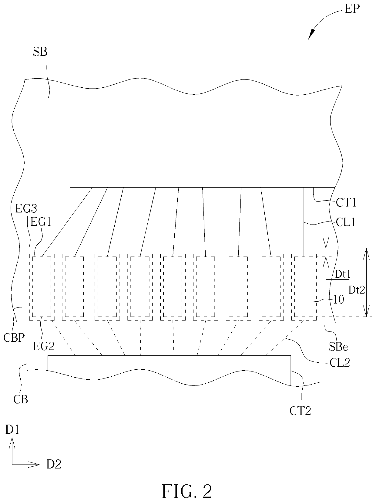
[0016]Referring to FIG. 1 to FIG. 4, FIG. 1 and FIG. 2 are top-view schematic diagrams illustrating a portion of an electronic product of a first e...


PUM

PropertyMeasurementUnit
lengthaaaaaaaaaa
transparentaaaaaaaaaa
transparent conductiveaaaaaaaaaa

Abstract

An electronic product includes a substrate and a bonding pad structure. The bonding pad structure is disposed on the substrate, and the bonding pad structure includes a first metal layer, a first insulating layer, at least one first connecting hole and a transparent conductive layer. The first metal layer and the first insulating layer are disposed on the substrate. The first connecting hole is situated in the first insulating layer, and the first connecting hole exposes a portion of the first metal layer. The transparent conductive layer is disposed on the first insulating layer, and the transparent conductive layer has a first edge and a second edge opposite to the first edge, wherein the transparent conductive layer is electrically connected to the first metal layer through the first connecting hole. A spacing between the first edge and the first connecting hole is greater than or equal to 100 μm.

Description

CROSS REFERENCE TO RELATED APPLICATION[0001]This application claims the priority benefit of China Patent Application Serial No. 201711456462.4, filed Dec. 28, 2017. The entirety of the above-mentioned patent application is hereby incorporated herein by reference and made a part of this specification.BACKGROUND OF THE INVENTION1. Field of the Invention[0002]The present invention relates to an electronic product, and more particularly to an electronic product having a bonding pad structure for reducing damage of water vapor.2. Description of the Prior Art[0003]Nowadays, electronic product has become an indispensable item in society. In the general electronic product, a bonding pad is disposed on a substrate, such that electronic structures (such as electronic devices, electronic modules and electronic components) can be electrically connected to each other through the bonding pad, and signals can be transmitted. For instance, the electronic product may be a display panel (or a touch d...

Claims


Application Information

Patent Timeline
Patent Type & Authority Patents(United States)
IPC IPC(8): H01L23/00H01L27/32H01L27/12
CPCH01L27/3276H01L27/1218H01L24/03H01L24/06H01L23/564H01L27/1248H01L24/05H01L24/08H01L2224/05084H01L2224/08225H01L2224/05024H01L2924/20641H01L27/124H01L27/1259H01L2224/05083H01L2224/06135H01L2224/0362H01L2224/05076H01L23/49811H01L23/49838H01L21/4846H10K59/131
Inventor LIU, HSUAN-CHENHSU, YU-TUAN
Owner HANNSTAR DISPLAY CORPORATION
Learn More