Dielectric device
a dielectric device and dielectric film technology, applied in the field of dielectric devices, can solve the problems of difficult enhancement of dielectric crystallinity and high manufacturing cost, and achieve the effect of increasing the throughput of deposition process and easy improvement of dielectric film crystallinity in the dielectric devi
- Summary
- Abstract
- Description
- Claims
- Application Information
AI Technical Summary
Benefits of technology
Problems solved by technology
Method used
Image
Examples
example 1
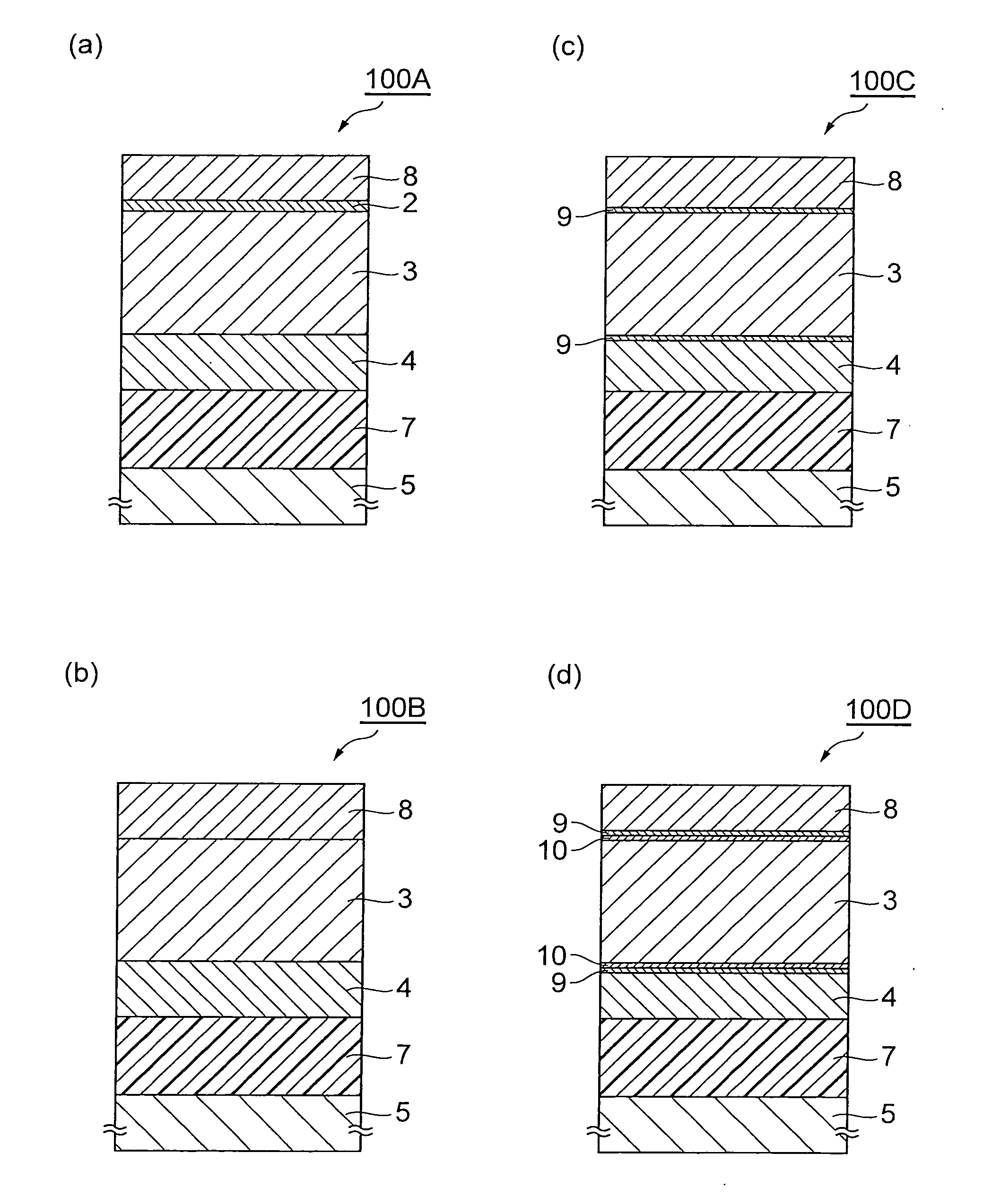
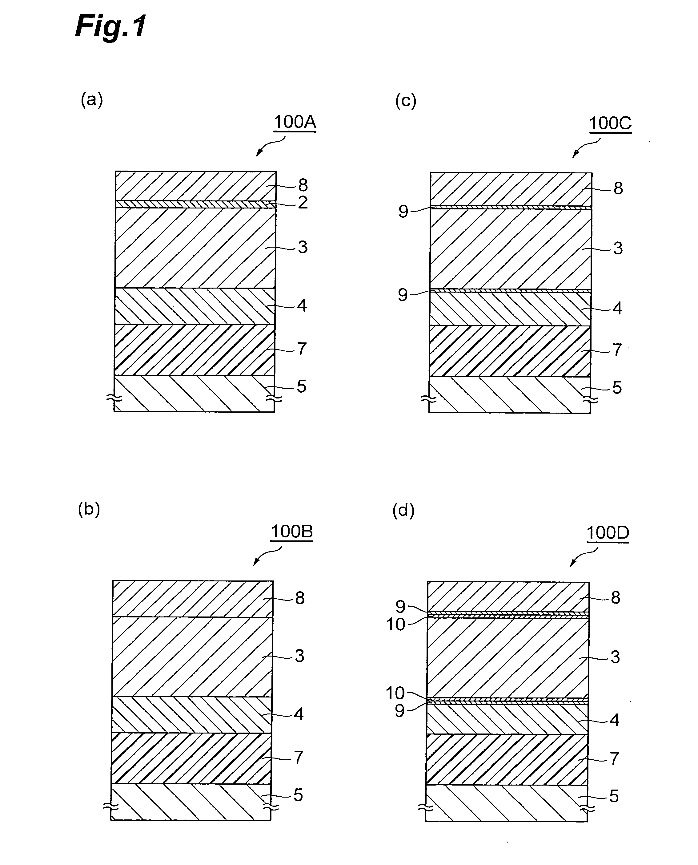
Dielectric Device 100A
[0090]In a state in which an Si substrate 1 was heated at 400° C., a Pt film was epitaxially grown in the thickness of 50 nm on the surface orientation of the Si substrate 1 by sputtering to obtain a (100) preferentially oriented metal film 2 on the Si substrate 1. A growth rate of the Pt film was 0.2 nm / sec. Thereafter, in a state in which the Si substrate 1 was heated at 550° C., a potassium sodium niobate (KNN) film was epitaxially grown as dielectric film 3 in the thickness of 2000 nm on the metal film 2 by sputtering to obtain a (110) preferentially oriented dielectric film 3. Subsequently, at room temperature, an Ni film was deposited in the thickness of 200 nm on the dielectric film 3 by sputtering to obtain an amorphous electrode film 4. Thereafter, the electrode film 4 was bonded to an Si support substrate 5 by an epoxy resin layer 7. Thereafter, the Si substrate 1 was removed from the metal film 2 by an etching process based on RIE. Then an Ni film wa...
example 2
Dielectric Device 100B
[0091]A dielectric device 100B was obtained in the same manner as in Example 1, except that the metal film 2 was also etched in addition to the Si substrate 1 in the removal of the Si substrate 1.
example 3
Dielectric Device 100C
[0092]A dielectric device 100C was obtained in the same manner as in Example 2, except that intermediate films 9 of a non-oriented structure composed of Ti were provided in the thickness of 5 nm between the dielectric film 3 and the two electrode films 4, 8 by sputtering. The dielectric device 100C was improved in adhesion of the dielectric film 3 to the electrode film 4 and the electrode film 8.
PUM
| Property | Measurement | Unit |
|---|---|---|
| thicknesses | aaaaa | aaaaa |
| thickness | aaaaa | aaaaa |
| oxidation-reduction potential | aaaaa | aaaaa |
Abstract
Description
Claims
Application Information


