
Dielectric device

a dielectric device and dielectric film technology, applied in the direction of capacitors, chemistry apparatus and processes, crystal growth processes, etc., can solve the problems of difficult enhancement of high manufacturing cost of the dielectric, so as to increase the throughput of the deposition process and improve the crystallinity of the dielectric film in the dielectric device.

Active Publication Date: 2018-03-15
TDK CORPARATION
View PDF0 Cites 0 Cited by
  • Summary
  • Abstract
  • Description
  • Claims
  • Application Information

AI Technical Summary

Benefits of technology

The present invention provides a dielectric device with improved crystallinity and lower manufacturing costs. By controlling the oxidation-reduction potential of the metal elements in the electrodes, a more stable dielectric film can be achieved. The electrode films are composed of metals with high oxidation-reduction potential, ensuring compatibility with the dielectric film. An electroconductive oxide film can also be added between the electrodes and the dielectric film to prevent device degradation. The invention allows for the replacement of expensive materials with inexpensive materials and increases the throughput of the deposition process.

Problems solved by technology

In the case of the conventional dielectric devices, however, it is not easy to enhance the crystallinity of the dielectric and manufacturing cost thereof is also high.

Method used


Image

  • Dielectric device
  • Dielectric device
  • Dielectric device

Examples


examples

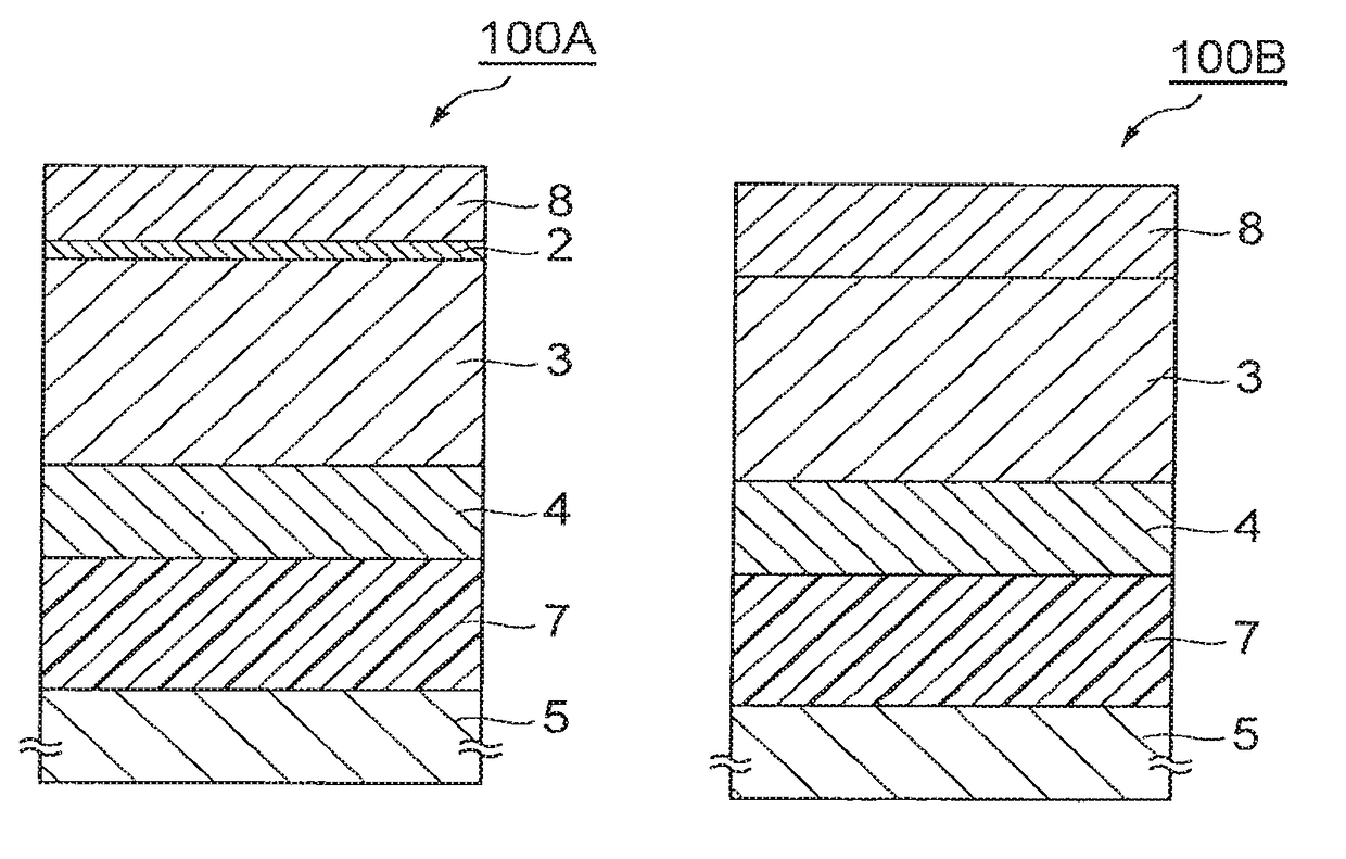
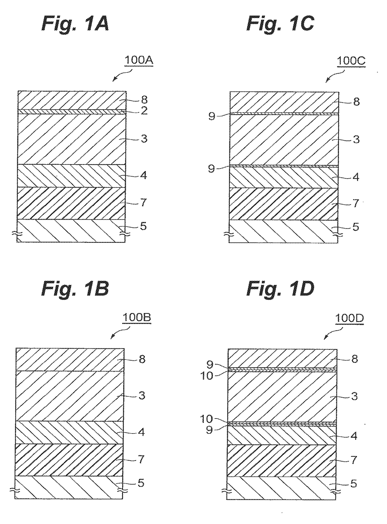
(Example 1) Dielectric Device 100A

[0089]In a state in which an Si substrate 1 was heated at 400° C., a Pt film was epitaxially grown in the thickness of 50 nm on the surface orientation of the Si substrate 1 by sputtering to obtain a (100) preferentially oriented metal film 2 on the Si substrate 1. A growth rate of the Pt film was 0.2 nm / sec. Thereafter, in a state in which the Si substrate 1 was heated at 550° C., a potassium sodium niobate (KNN) film was epitaxially grown as dielectric film 3 in the thickness of 2000 nm on the metal film 2 by sputtering to obtain a (110) preferentially oriented dielectric film 3. Subsequently, at room temperature, an Ni film was deposited in the thickness of 200 nm on the dielectric film 3 by sputtering to obtain an amorphous electrode film 4. Thereafter, the electrode film 4 was bonded to an Si support substrate 5 by an epoxy resin layer 7. Thereafter, the Si substrate 1 was removed from the metal film 2 by an etching process based on RIE. Then a...

experimental examples

Other Experimental Examples

[0097]With change in film thickness of the metal film 2 deposited on the single-crystal Si substrate, the orientation of the dielectric film 3 deposited thereon was measured every time by X-ray diffractometry (XRD) with the aforementioned diffractometer. The epitaxial metal film 2 was formed by DC sputtering under the conditions of surface orientation of single-crystal Si substrate 1: (100), composition of metal film 2: Pt (2-200 nm) film, substrate temperature during deposition: 400° C., gas pressure: 0.10 Pa, and input power 150 W. The deposition rate was 0.2 nm / sec.

[0098]The dielectric film 3 was formed on the metal film 2 by DC sputtering under the conditions of composition of dielectric film 3: potassium sodium niobate, substrate temperature: 550° C., gas pressure: 0.15 Pa, and input power: 700 W. The film thickness was 2000 nm. For each of samples in which the films up to the dielectric film 3 were deposited, a percentage of the peak intensity ascrib...


PUM

PropertyMeasurementUnit
thicknessaaaaaaaaaa
thicknessaaaaaaaaaa
oxidation-reduction potentialaaaaaaaaaa

Abstract

A dielectric device has a first electrode film having a non-oriented or amorphous structure, a dielectric film provided on the first electrode film and having a preferentially oriented structure, and a second electrode film provided on the dielectric film and having a non-oriented or amorphous structure.

Description

[0001]This is a Continuation of application Ser. No. 13 / 487,530 filed Jun. 4, 2012. The disclosure of the prior application is hereby incorporated by reference herein in its entirety.BACKGROUND OF THE INVENTIONField of the Invention[0002]The present invention relates to a dielectric device.Related Background Art[0003]There are conventionally known dielectric devices having a dielectric film and a pair of electrode films laid on both sides of the dielectric film, as disclosed in Patent Literatures 1 to 5.[0004]Patent Literature 1: Japanese Patent Application Laid-open No. 2010-103194[0005]Patent Literature 2: Japanese Patent Application Laid-open No. 2009-094449[0006]Patent Literature 3: Japanese Patent Application Laid-open No. 2008-211385[0007]Patent Literature 4: Japanese Patent Application Laid-open No. 2007-277606[0008]Patent Literature 5: Japanese Patent Application Laid-open No. 2006-286911SUMMARY OF THE INVENTION[0009]In the case of the conventional dielectric devices, howeve...

Claims


Application Information

Patent Timeline
Patent Type & Authority Applications(United States)
IPC IPC(8): H01L41/08H01L41/047H10N30/06H10N30/00H10N30/87H10N30/071H10N30/072H10N30/074H10N30/079H10N30/09H10N30/80H10N30/853H10N97/00
CPCH01L41/0477H01L41/0815H10N30/877H10N30/708C30B23/02Y10T29/42H01L28/55H10N30/06H10N30/09H10N30/071H10N30/072H10N30/074
Inventor KURACHI, KATSUYUKISAKUMA, HITOSHIAIDA, YASUHIROMAEJIMA, KAZUHIKONAKAJIMA, MAYUMI
Owner TDK CORPARATION
Learn More