Supercharge Your Innovation With Domain-Expert AI Agents!

Electroluminescent display device

a display device and electroluminescent technology, applied in the direction of electroluminescent light sources, solid-state devices, electric lighting sources, etc., can solve the problems of difficult application of vacuum thermal evaporation process to a display device of a large area and high resolution, increased manufacturing costs, and inability to achieve uniform evaporation within the pixel area. , to achieve the effect of reducing the area and resolution, increasing the manufacturing cos

Active Publication Date: 2020-05-26
LG DISPLAY CO LTD
View PDF18 Cites 6 Cited by
  • Summary
  • Abstract
  • Description
  • Claims
  • Application Information

AI Technical Summary

Benefits of technology

The present invention provides an electroluminescent display device that solves problems related to increased manufacturing cost and area limitations due to the evaporation process. Additionally, it improves image quality.

Problems solved by technology

However, such a vacuum thermal evaporation method has problems in that the manufacturing cost is increased by the mask and it is difficult to apply the vacuum thermal evaporation process to a display device of a large area and high resolution due to manufacturing deviation of the mask, deflection, shadow effect, etc.
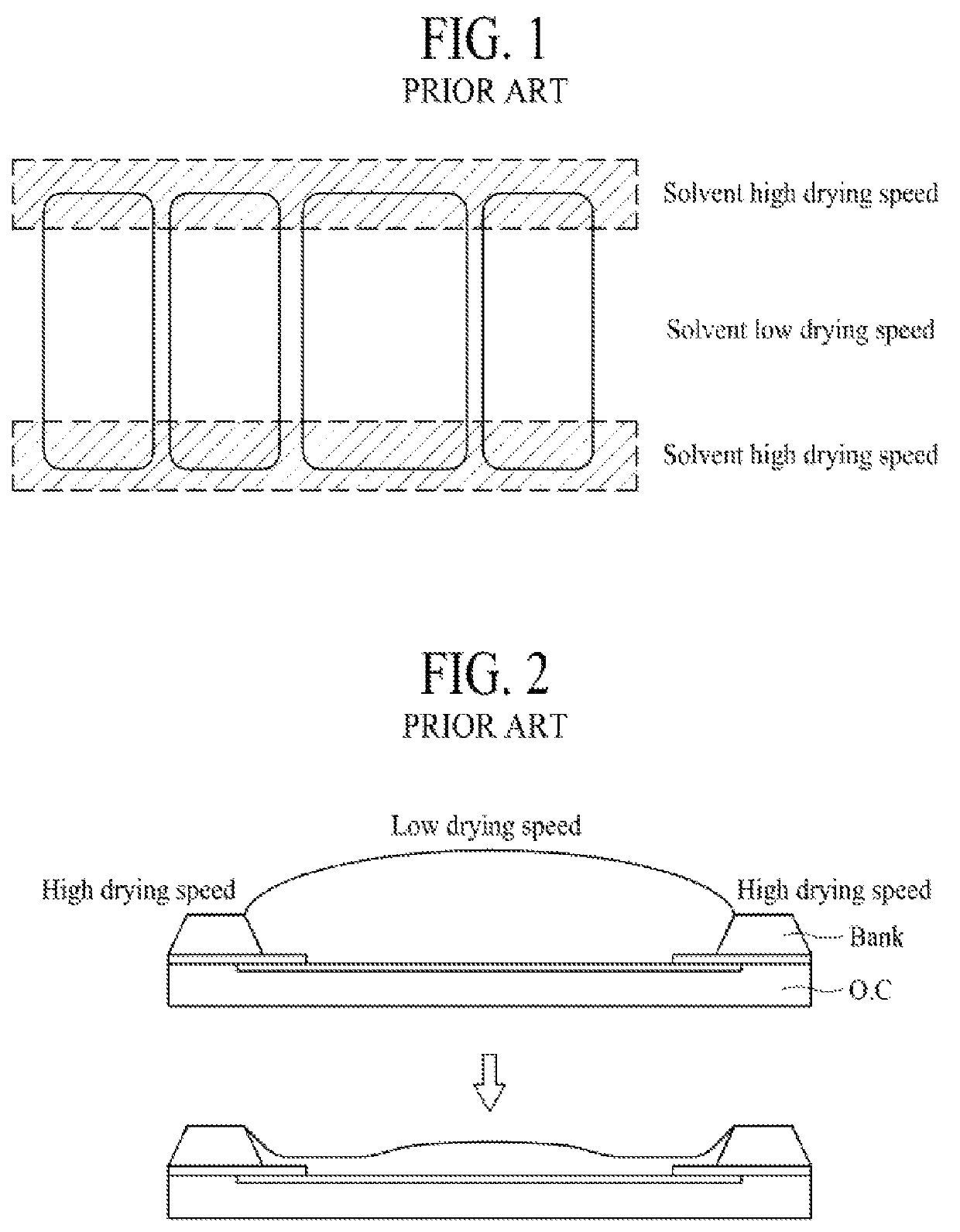
On the other hand, if the light emitting layer is formed using the ink jet device, solvent evaporation within the pixel area is not carried out uniformly during the drying process, whereby a problem occurs in that a thickness of the light emitting material layer does not become uniform.
As shown in FIG. 1, evaporation of a solvent is not carried out uniformly within a pixel area during a drying process of a solution.
For this reason, light emission is not uniform, and luminance of the electroluminescent display device is not uniform, whereby image quality is deteriorated.

Method used


Image

  • Electroluminescent display device
  • Electroluminescent display device
  • Electroluminescent display device

Examples


Embodiment Construction

[0030]Terms disclosed in this specification should be understood as follows.

[0031]The term of a singular expression should be understood to include multiple expressions as well as the singular expression if there is no specific definition in the context. The terms such as “the first” and “the second” are used only to differentiate one element from other elements. Thus, a scope of claims is not limited by these terms. Also, it should be understood that the term such as “include” or “have” does not preclude existence or possibility of one or more features, numbers, steps, operations, elements, parts or their combinations. It should be understood that the term “at least one” includes all combinations related with any one item. For example, “at least one among a first element, a second element and a third element” may include all combinations of two or more elements selected from the first, second and third elements as well as each element of the first, second and third elements. Also, ...


PUM

PropertyMeasurementUnit
areaaaaaaaaaaa
widthaaaaaaaaaa
depthaaaaaaaaaa

Abstract

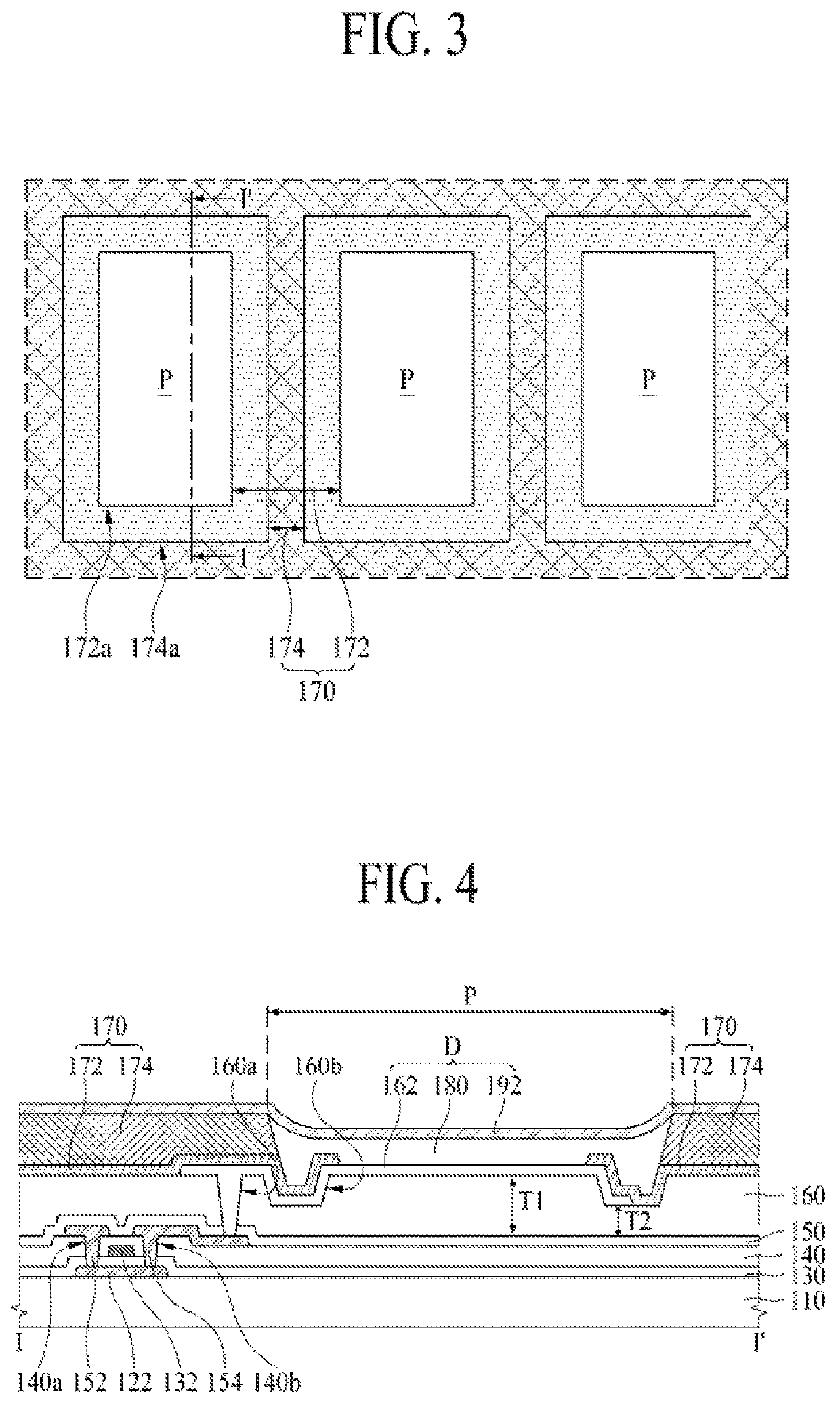
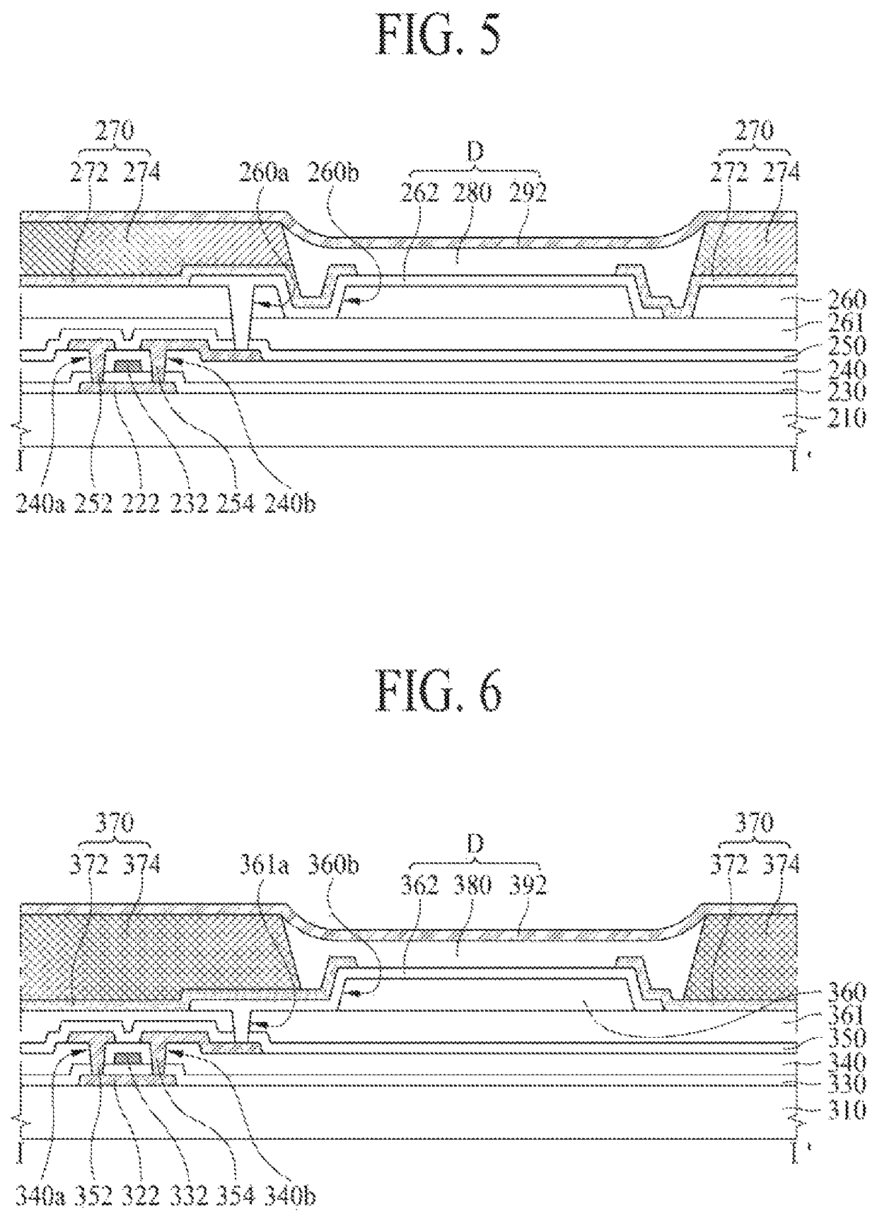
An electroluminescent display device which may improve display quality is discussed. The electroluminescent display device includes a substrate in which a plurality of pixel areas are defined, a first electrode arranged in each pixel area, a light emitting layer on the first electrode within the pixel area, and a second electrode on the light emitting layer. Particularly, a step difference portion is arranged at an edge of the pixel area, and is partially or fully be filled with the light emitting layer. Film uniformity of the light emitting layer within the pixel area may be improved by arrangement of the step difference portion.

Description

CROSS REFERENCE TO RELATED APPLICATIONS[0001]This application claims the priority benefit of the Korean Patent Application No. 10-2016-0179272 filed on Dec. 26, 2016 in the Republic of Korea, the disclosure of which is hereby incorporated by reference in its entirety.BACKGROUND OF THE INVENTIONField of the Invention[0002]Embodiments of the present invention relate to an electroluminescent display device, and more particularly, to an electroluminescent display device of a large area, which may provide uniform luminance.Discussion of the Related Art[0003]Recently, flat panel displays having excellent characteristics such as thin profile, light weight, and low power consumption have been widely developed and applied to various fields.[0004]Among the flat panel displays, an electroluminescent display device is a device that emits light by means of radiative recombination of exciton formed by electrons and holes by injecting charges into a light emitting layer formed between a cathode wh...

Claims


Application Information

Patent Timeline
Patent Type & Authority Patents(United States)
IPC IPC(8): H01L51/52H05B33/08H01L27/32H05B33/26H05B33/10H05B33/20H05B33/22H05B44/00
CPCH05B33/08H05B33/10H01L51/5203H01L51/5209H05B33/20H01L27/3246H05B33/22H05B33/26H01L27/3258H10K59/122H10K59/8051H10K59/873H10K59/8052H10K59/124H10K59/35H10K50/11H10K2102/351H10K50/805H10K50/813
Inventor PARK, KYOUNGJINKIM, HANHEEYANG, KISOUBJEON, HONGMYEONGJUNG, SUNGGOO
Owner LG DISPLAY CO LTD
Features
  • R&D
  • Intellectual Property
  • Life Sciences
  • Materials
  • Tech Scout
  • Unparalleled Data Quality
  • Higher Quality Content
  • 60% Fewer Hallucinations
Learn More