Polishing compositions
a technology of composition and polishing composition, which is applied in the direction of lapping machines, manufacturing tools, other chemical processes, etc., can solve the problems of difficult to form multi-filmed wiring in semiconductor devices, difficult to remove conductive films to an excessive degree, and difficult to form multi-filmed wiring, etc., to achieve reduced dr, reduce dr, and reduce the effect of dr
Active Publication Date: 2020-07-14
FUJIFILM ELECTRONICS MATERIALS US
View PDF11 Cites 0 Cited by
- Summary
- Abstract
- Description
- Claims
- Application Information
AI Technical Summary
Benefits of technology
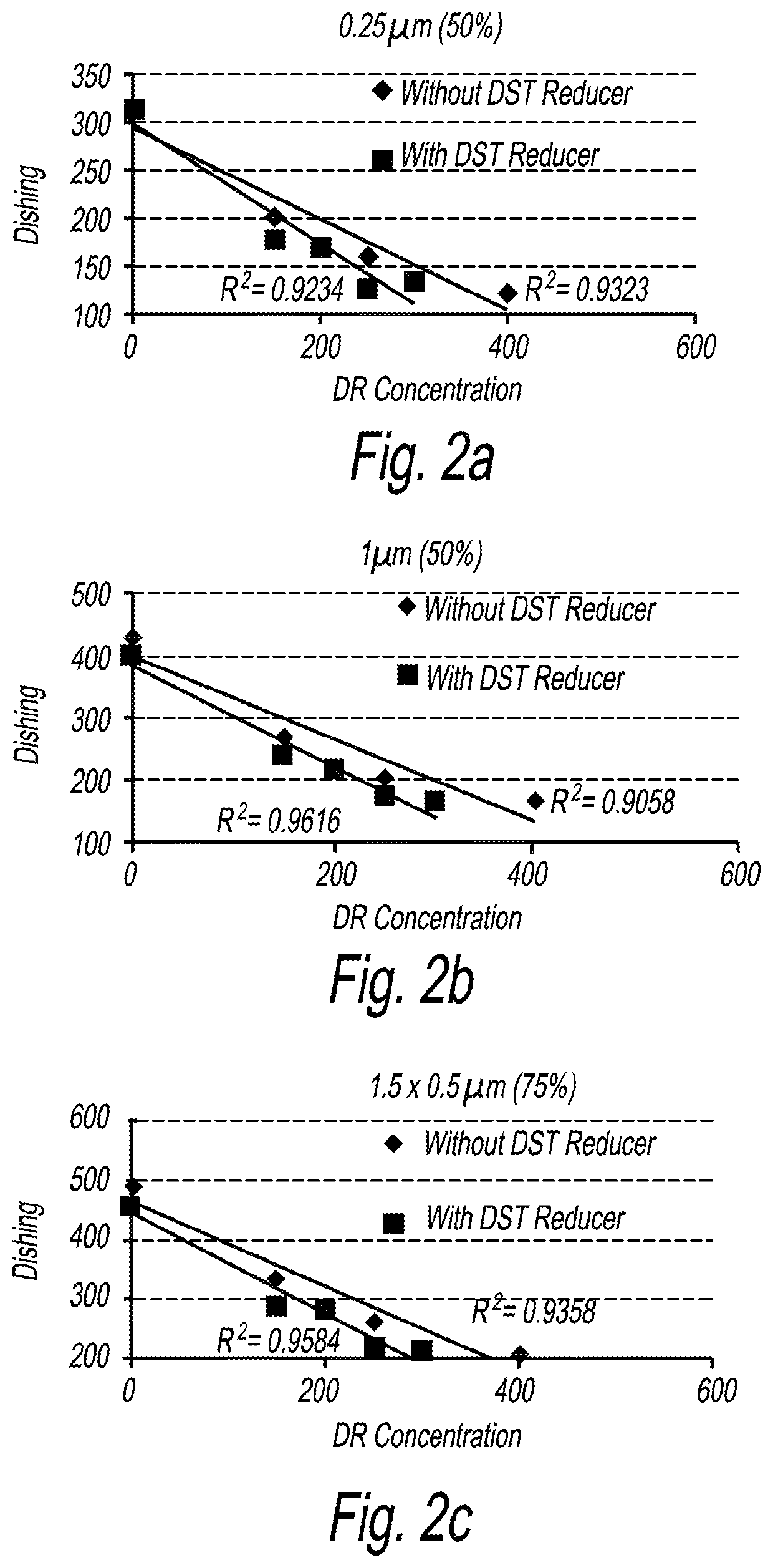
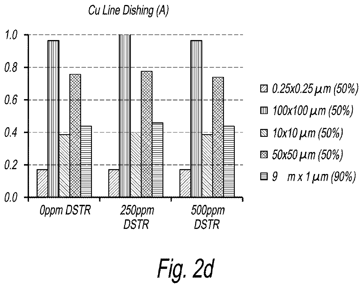
These compositions achieve minimal dishing and high removal rates with lower DR concentrations, reducing copper residue and maintaining surface quality, as demonstrated by the synergistic effect of DR and DSTR, which enhances the polishing process efficiency and throughput.
Problems solved by technology
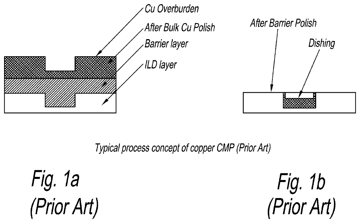
This is thought to be attributed to removal of the conductive films to an excessive degree, due to an excessively high ability of each of the first conventional polishing composition to polish the copper containing metal.
The dishing also impairs the flatness of the surface of a semiconductor device, thereby making it difficult to form multi-filmed wiring in the semiconductor device.
Although this approach has met with some success, copper residue remaining on the wafer can be problematic when the concentration of dishing reducer is too high.
Method used
View moreImage
Smart ImageViewing Examples
Examples
examples
[0093]The following formulation is a typical composition contemplated for use in the practice of the disclosure. All values are in wt %. The amounts shown are for a concentrate, which at POU is diluted by a factor of 10.
[0094]
Formula 1Complexing agent 0.1-20Silica 0.01-10Azole 10.001-5 DR0.001-0.1DSTR0.001-0.1Azole 20.001-5 pH 4-9Dilution Ratio10
Login to View More PUM
| Property | Measurement | Unit |
|---|---|---|
| thickness | aaaaa | aaaaa |
| defect sizes | aaaaa | aaaaa |
| composition | aaaaa | aaaaa |
Abstract
The present disclosure provides chemical mechanical polishing compositions that achieve minimal dishing at reduced dishing reducer (DR) levels when compared to known CMP compositions. The compositions of the disclosure include a dynamic surface tension reducer (DSTR) which allows for lower levels of dishing reducer in the compositions. Indeed, the compositions of the disclosure allow for lower levels of dishing reducer to achieve the same dishing as known compositions having higher levels of dishing reducer. Deleterious effects of high DR levels are thereby avoided or minimized when employing the compositions of the disclosure.
Description
CROSS-REFERENCE TO RELATED APPLICATION[0001]The present application claims the benefit of U.S. Provisional Application Ser. No. 62 / 440,649, filed on Dec. 30, 2016, which is herein incorporated by reference.BACKGROUND OF THE DISCLOSURE[0002]1. Field of the Disclosure[0003]The present disclosure relates generally to polishing compositions, and methods for polishing semiconductor substrates using the compositions described herein. More particularly, the disclosure relates to chemical mechanical polishing compositions and methods for removing copper layers from a semiconductor substrate, where the compositions include synergistic combinations of surfactants.[0004]2. Description of the Related Art[0005]The process known as chemical-mechanical polishing (CMP) involves polishing different metal or non-metal layers on semiconductor wafers, using a polish pad and slurry. Copper is a commonly used material for forming interconnects in semiconductor manufacturing. Once a copper inlaid structur...
Claims
Login to View More Application Information
Patent Timeline
 Patent Type & Authority Patents(United States)
IPC IPC(8): C09G1/02C23F3/04B24B37/04H01L21/321H01L21/768
CPCC09G1/02C23F3/04H01L21/3212B24B37/044H01L21/7684H01L21/30625C09K3/14
Inventor MCDONOUGH, JAMES
Owner FUJIFILM ELECTRONICS MATERIALS US


