Semiconductor package

a technology of semiconductor chips and components, applied in the direction of semiconductor devices, semiconductor/solid-state device details, electrical apparatus, etc., can solve the problems of increasing electrical noise, reduce process defects, reduce electrical path, reduce semiconductor chip mounting area, effect of reducing process defects

Active Publication Date: 2020-07-28
SAMSUNG ELECTRONICS CO LTD
View PDF23 Cites 87 Cited by
  • Summary
  • Abstract
  • Description
  • Claims
  • Application Information

AI Technical Summary

Benefits of technology

[0005]An aspect of the present disclosure is to provide a semiconductor package having a novel structure that significantly reduces the mounting area of the semiconductor chip and the passive components, significantly reduces the electrical path between the semiconductor chip and the passive components, significantly reduces process defects such as undulations and cracks, and easily connects the electrodes of the passive components to connection vias by a laser-via hole process or the like.

Problems solved by technology

This may be cost effective, but there can be problems in that a large mounting area is required due to the minimum interval between components, relatively high electromagnetic interference (EMI) between components, and a relatively larger distance between the semiconductor chip and the passive components, which can increase electrical noise.

Method used


Image

  • Semiconductor package
  • Semiconductor package
  • Semiconductor package

Examples


Embodiment Construction

[0030]Hereinafter, embodiments of the present disclosure will be described as follows with reference to the attached drawings. The shape and size of elements in the drawings may be exaggerated or reduced for clarity.

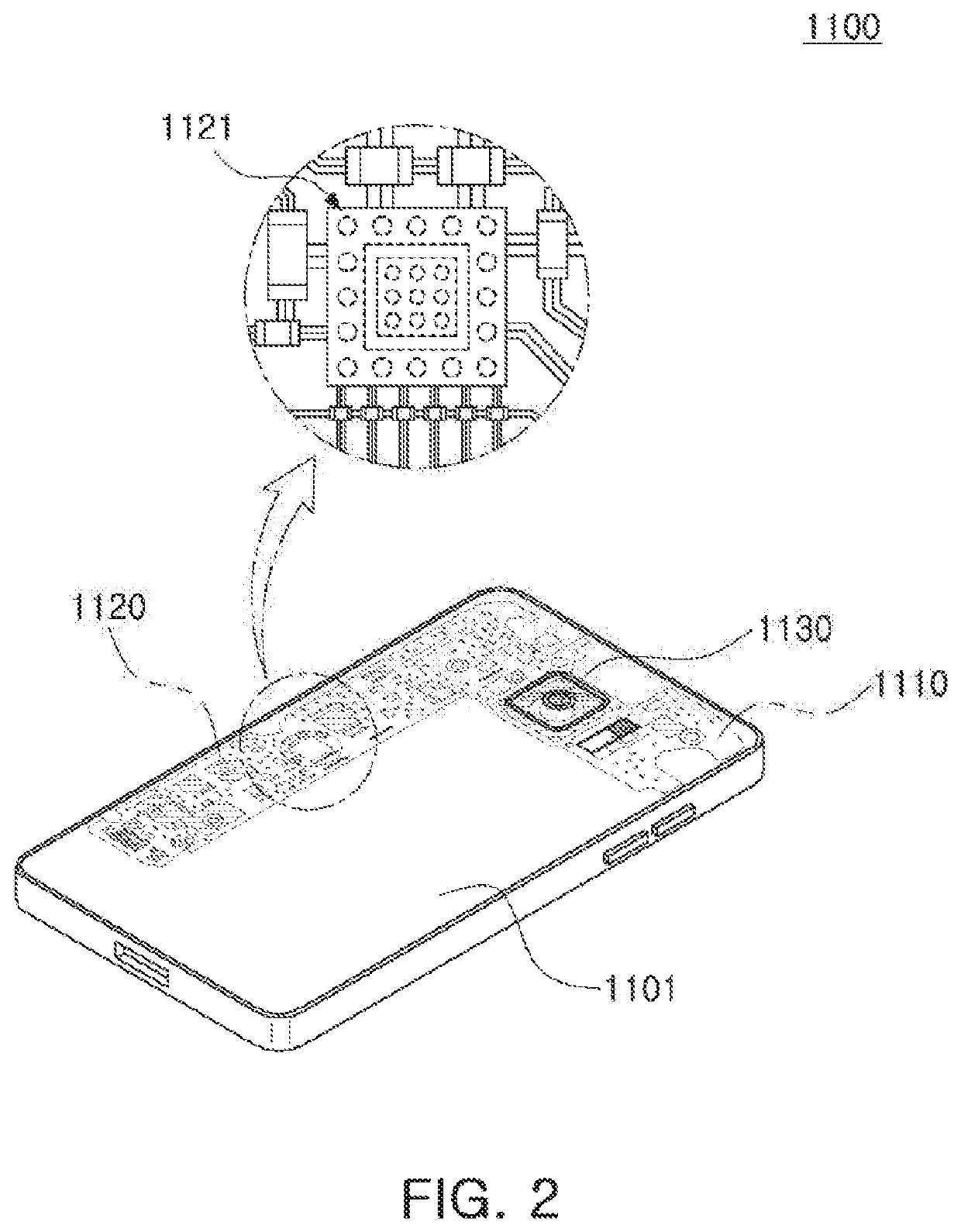
[0031]Electronic Device

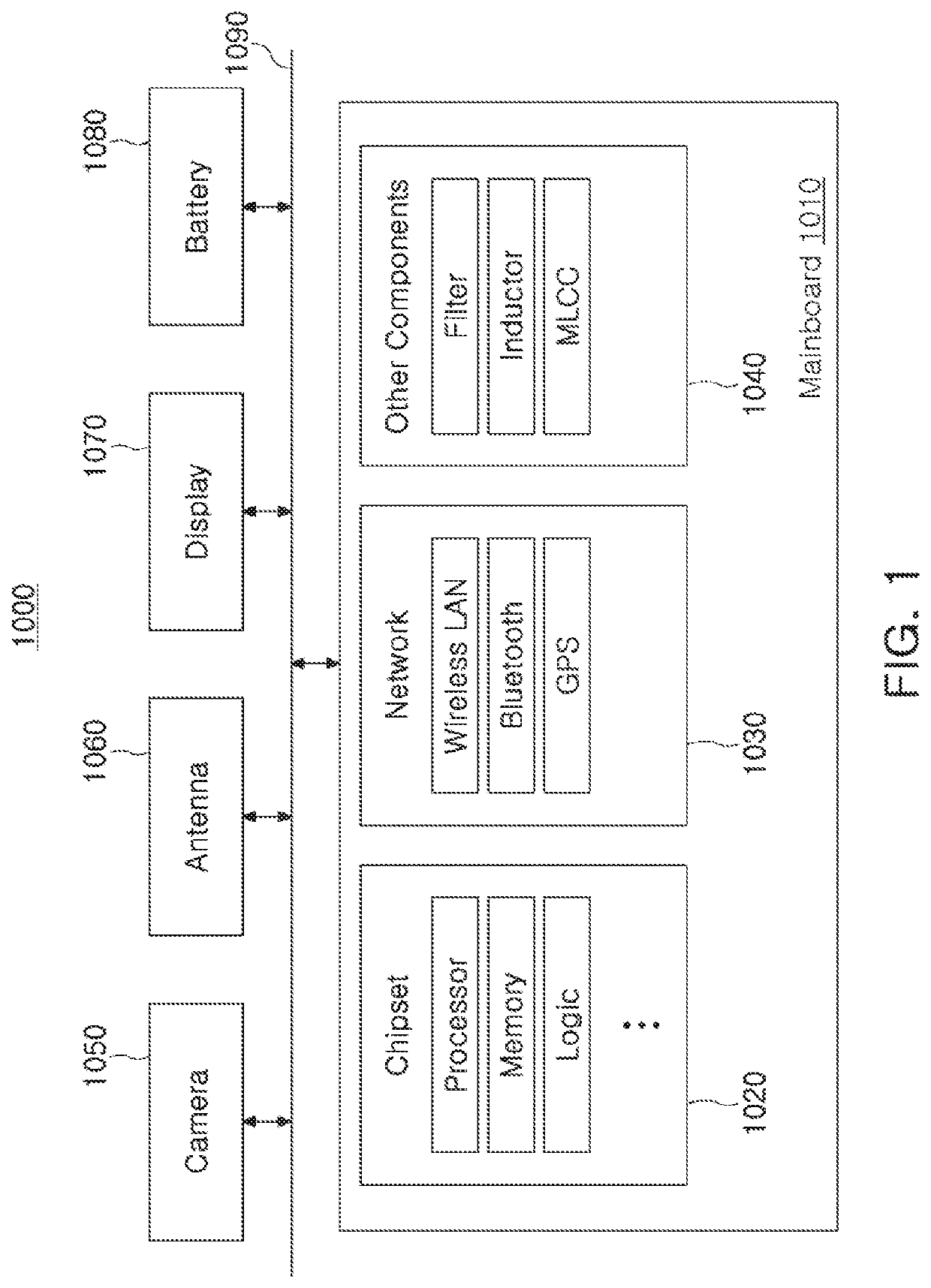
[0032]FIG. 1 is a block diagram schematically illustrating an exemplary embodiment of an electronic device system.

[0033]Referring to the drawings, an electronic device 1000 may include a main board 1010. The main board 1010 may be physically and / or electrically connected to chip-related components 1020, network-related components 1030, and other components 1040. They may be also combined with other components to be described later to form various signal lines 1090.

[0034]The chip-related components 1020 may include a memory chip, such as a volatile memory (e.g., DRAM), a non-volatile memory (e.g., ROM), a flash memory, etc.; an application processor chip, such as a central processor (e.g., CPU), a graphics processor (e.g., GPU), a digital signal pro...


PUM

PropertyMeasurementUnit
thicknessaaaaaaaaaa
coefficient of thermal expansionaaaaaaaaaa
CTEaaaaaaaaaa

Abstract

A semiconductor package includes a connection structure including a first insulation layer, a second insulation layer, first and second wiring layers, and first and second connection vias. A core structure including a core member is on the first insulation layer. A first through-hole passes through the core member. Passive components are on the first insulation layer in the first through-hole and connected to the first wiring layer through the first connection via. A first encapsulant covers at least a portion of the passive components. A second through-hole passes through the core structure and the first insulation layer. A semiconductor chip is on the second insulation layer in the second through-hole and is connected to the second wiring layer through the second connection via. A second encapsulant covers at least a portion of the semiconductor chip.

Description

CROSS-REFERENCE TO RELATED APPLICATIONS[0001]This application claims benefit of priorities to Korean Patent Application No. 10-2018-0030337 filed on Mar. 15, 2018, and Korean Patent Application No. 10-2018-0070111 filed on Jun. 19, 2018, in the Korean Intellectual Property Office, the disclosures of which are incorporated herein by reference in their entireties.BACKGROUND1. Field[0002]The present disclosure relates to a semiconductor package modularized by mounting a semiconductor chip together with a plurality of passive components in a single package.2. Description of Related Art[0003]As the size of mobile device displays increase, there has been a need for increasing battery capacity. As battery capacity increases, the area occupied by the battery increases. As a result, the size of the printed circuit board PCB must be reduced, such that mounting areas for components are reduced and interest in modularization is continuously increasing.[0004]Conventional technology for mounting ...

Claims


Application Information

Patent Timeline
Patent Type & Authority Patents(United States)
IPC IPC(8): H01L23/498H01L25/16H01L23/053H01L23/31H01L21/52H01L21/56H01L21/48H01L23/00
CPCH01L21/56H01L21/4857H01L23/49822H01L23/49827H01L21/52H01L25/16H01L23/3128H01L23/49894H01L23/49838H01L24/08H01L23/3135H01L23/053H01L2224/08235H01L21/50H01L21/6836H01L21/6835H01L2221/68345H01L2221/68372H01L21/568H01L2224/18H01L23/5389H01L23/50H01L23/49816H01L24/19H01L24/20H01L23/552
Inventor MOON, SEON HEEKANG, MYUNG SAMKO, YOUNG GWANLEE, CHANG BAEKIM, JIN SU
Owner SAMSUNG ELECTRONICS CO LTD
Why Eureka
Try Eureka