Component with geometrically adapted contact structure and method for producing the same

a contact structure and geometrically adapted technology, applied in the direction of semiconductor devices, electrical devices, semiconductor/solid-state device details, etc., can solve the problems of unreliable connection, large risk of components being damaged, and between components, and achieve the effect of simple and reliable mechanical connection

Active Publication Date: 2020-08-11
OSRAM OPTO SEMICON GMBH & CO OHG
View PDF14 Cites 0 Cited by
  • Summary
  • Abstract
  • Description
  • Claims
  • Application Information

AI Technical Summary

Benefits of technology

[0004]Embodiments provide a component with a geometrically adapted contact structure that allows a simplified and reliable mechanical connection to another component. Further embodiments provide a simplified method for producing such a component.
[0006]The predetermined geometrically non-planar contour profile can be given by the contour profile of one layer of the component or by a mounting surface or by a connecting surface of a further component. The contacts having at least in part different vertical heights are adapted to a predetermined geometrically non-planar contour profile, such as to a contour profile having a non-planar, in particular curved surface if the contacts have ends whose surfaces define a contour profile which substantially reproduces the predetermined geometrically non-planar contour profile. Here, the ends of the contacts can face towards or face away from the mounting surface of the component. In particular, the one ends of the contacts define a flat surface, while the other opposite ends of the contacts define a non-planar, in particular curved, surface. By combining the heights of the contacts with their lateral positions, possible deformations of the component are compensated by the contour profile of the contacts. The height-compensation allows, for example, to better follow a given contour profile of a curved surface. The height-compensation also makes it possible for the component to have a mounting surface having the highest standards in terms of evenness. Thus, the height-compensation enables a more reliable connection, especially at the edge of the component, which results in a higher yield and more robust components.

Problems solved by technology

Thermomechanical tension between different functional levels of the component often leads to undesired deformations—also known as “bowling”—resulting in an unreliable connection, such as an unreliable solder connection, between the components.
The deformations can be grinded flat, but there is a great risk that the components will be damaged.
However, such methods prove to be costly and often not sufficiently reliable.

Method used


Image

  • Component with geometrically adapted contact structure and method for producing the same
  • Component with geometrically adapted contact structure and method for producing the same
  • Component with geometrically adapted contact structure and method for producing the same

Examples


Embodiment Construction

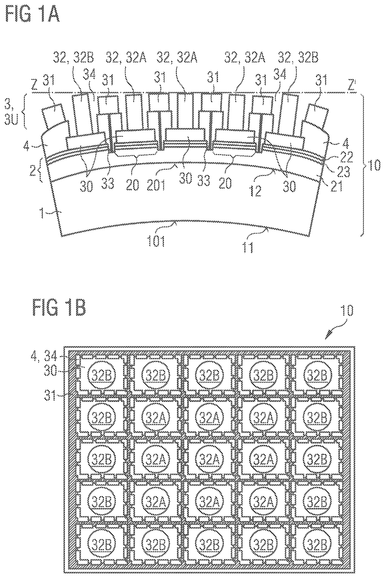
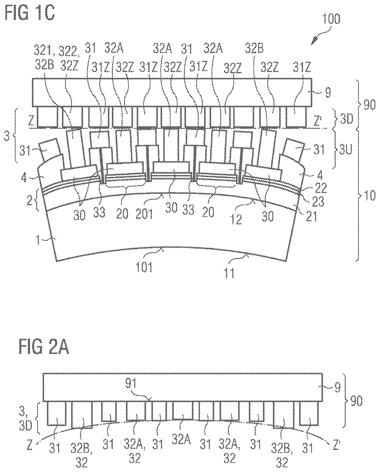
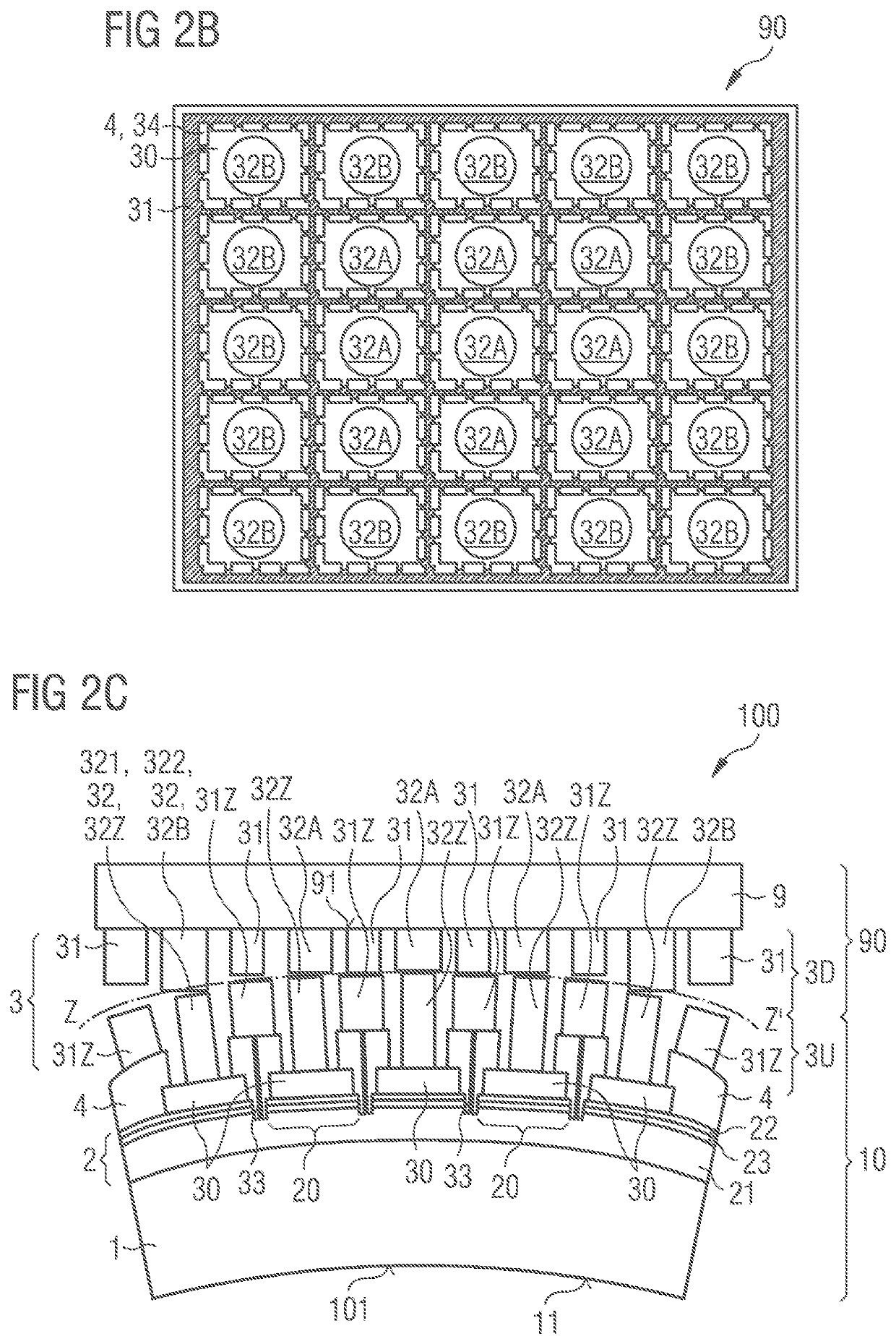
[0046]An exemplary embodiment of a component 10 is shown schematically in FIG. 1A in a sectional view. In FIG. 1B, the component 10 as shown in FIG. 1A is shown schematically in a plan view of a connecting surface ZZ′. The component 10 has a carrier 1 and a semiconductor body 2 arranged on the carrier. The carrier 1 can be a growth substrate on which the semiconductor body 2 is grown epitaxially in layers. However, the carrier 1 may be different from a growth substrate or from a grinded growth substrate. For example, the carrier 1 is a silicon or sapphire substrate. The component 10 has a contact structure 3 or 3U on a surface of the semiconductor body 2 facing away from the carrier 1. Connection layers 30 are arranged between the contact structure 3 and the semiconductor body 2. The connection layers 30 are especially laterally spaced apart. In particular, the connection layers 30 define a plurality of pixels formed by subregions 20 of the semiconductor body 2. In particular, the c...


PUM


Abstract

A component with an geometrically adapted contact structure and a method for producing such a component are disclosed. In an embodiment a component includes a contact structure including a contiguous contact layer having a plurality of openings and being assigned to a first electrical polarity of the component and a plurality of individual contacts at least in part having different vertical heights, wherein the contacts extend in the openings throughout the contiguous contact layer, wherein the contacts are laterally spaced from each other and assigned to a second electrical polarity of the component, and wherein the contacts are arranged with respect to their different heights and their positions such that a height distribution of the contacts is adapted to a predetermined geometrically non-planar contour profile.

Description

[0001]This patent application is a national phase filing under section 371 of PCT / EP2017 / 067695, filed Jul. 13, 2017, which claims the priority of German patent application 102016113193.8, filed Jul. 18, 2016, each of which is incorporated herein by reference in its entirety.TECHNICAL FIELD[0002]A component with a geometrically adapted contact structure is specified. Furthermore, a method for producing a component with a geometrically adapted contact structure is specified.BACKGROUND[0003]In the case of hetero-integration of components, in particular with a plurality of light dots, a reliable connection of the light dots to a driver circuit is necessary. Thermomechanical tension between different functional levels of the component often leads to undesired deformations—also known as “bowling”—resulting in an unreliable connection, such as an unreliable solder connection, between the components. The deformations can be grinded flat, but there is a great risk that the components will b...

Claims


Application Information

Patent Timeline
Patent Type & Authority Patents(United States)
IPC IPC(8): H01L33/38H01L23/00H01L33/20H01L33/08H01L33/24
CPCH01L33/20H01L24/17H01L24/13H01L24/16H01L33/24H01L33/382H01L24/81H01L33/08H01L33/387H01L24/14H01L2224/13007H01L2224/0401H01L2224/05624H01L2224/16111H01L2224/13021H01L2224/05639H01L2224/13019H01L2224/16147H01L2224/06102H01L2224/171H01L2224/81193H01L2224/13023H01L2224/141H01L2224/14051H01L2224/1403H01L2224/16148H01L2224/81815H01L2224/13022H01L2224/14104H01L2924/00014H01L2924/00012H01L2924/3511H01L2224/05567
Inventor PFEUFFER, ALEXANDER F.
Owner OSRAM OPTO SEMICON GMBH & CO OHG
Why Eureka
Try Eureka