Supercharge Your Innovation With Domain-Expert AI Agents!

Module

a module and module technology, applied in the field of modules, can solve the problems that the circuit module b>100/b> cannot achieve a sufficiently high level of mounted component integration, and achieve the effects of suppressing breakage in the circuit board, increasing the freedom with which the layout can be designed, and increasing the level of component integration

Active Publication Date: 2020-11-24
MURATA MFG CO LTD
View PDF23 Cites 0 Cited by
  • Summary
  • Abstract
  • Description
  • Claims
  • Application Information

AI Technical Summary

Benefits of technology

The patent text describes a circuit module that can help reduce interference between components caused by unnecessary electromagnetic waves. However, the module cannot achieve a high level of integration for the components. The present disclosure provides an improved module that can achieve better component integration while also reducing interference.

Problems solved by technology

However, although the above-described circuit module 100 can reduce interference caused by unnecessary electromagnetic waves between the mounted component 102a and the mounted component 102b, the circuit module 100 cannot achieve a sufficiently high level of mounted component integration.

Method used


Image

  • Module
  • Module
  • Module

Examples


first embodiment

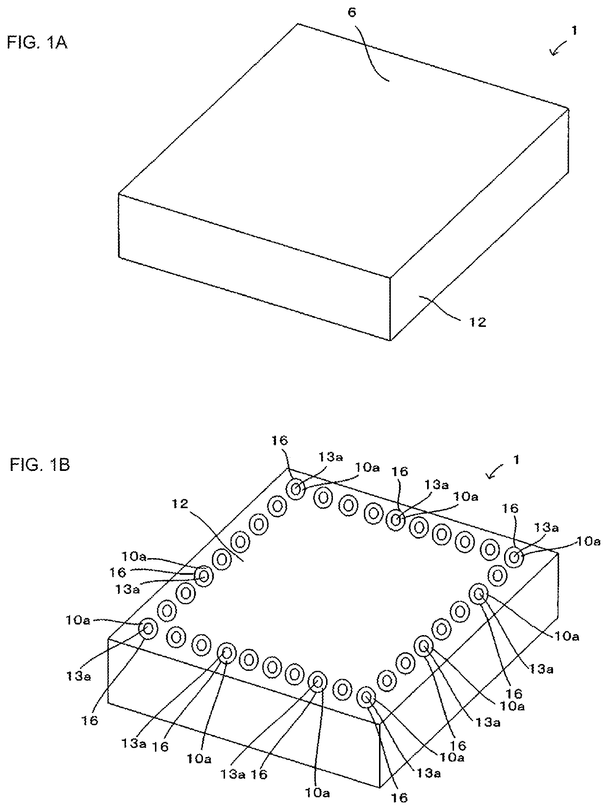
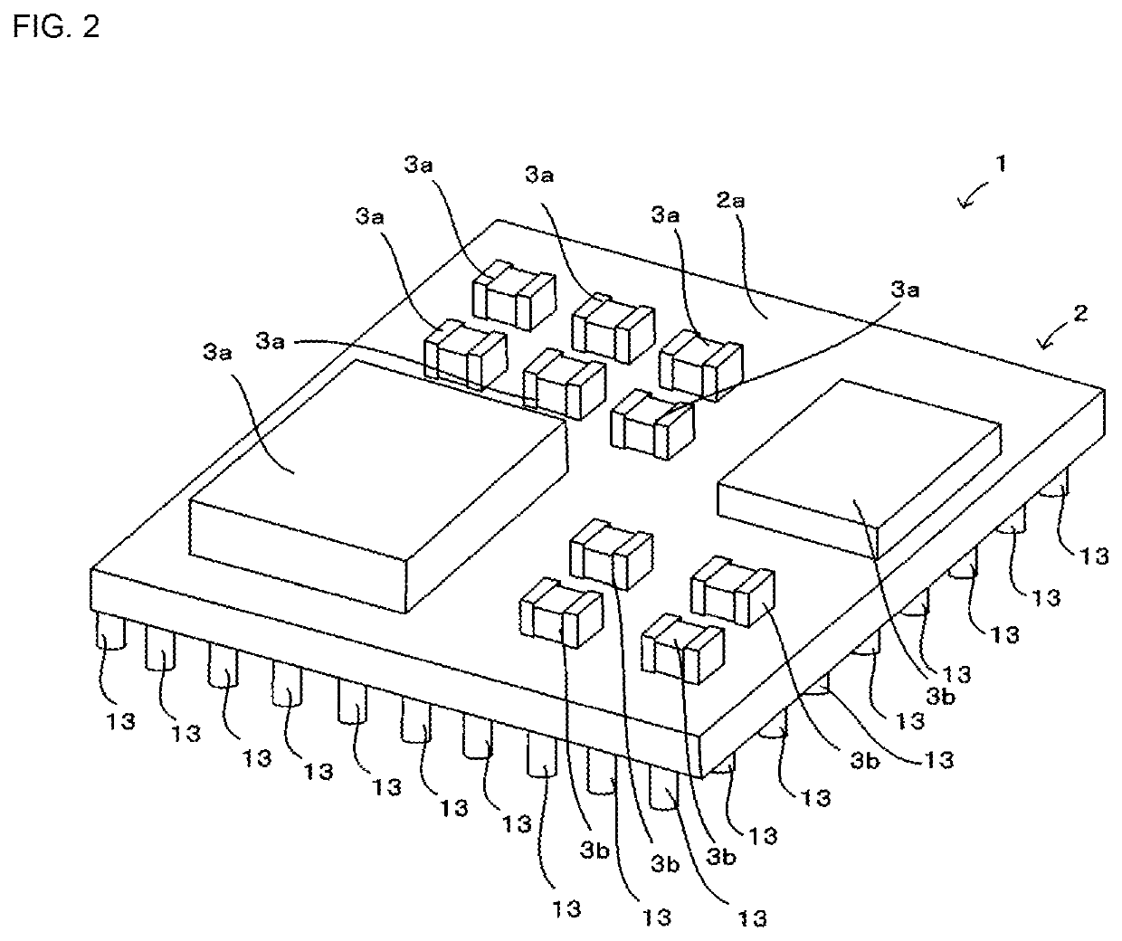
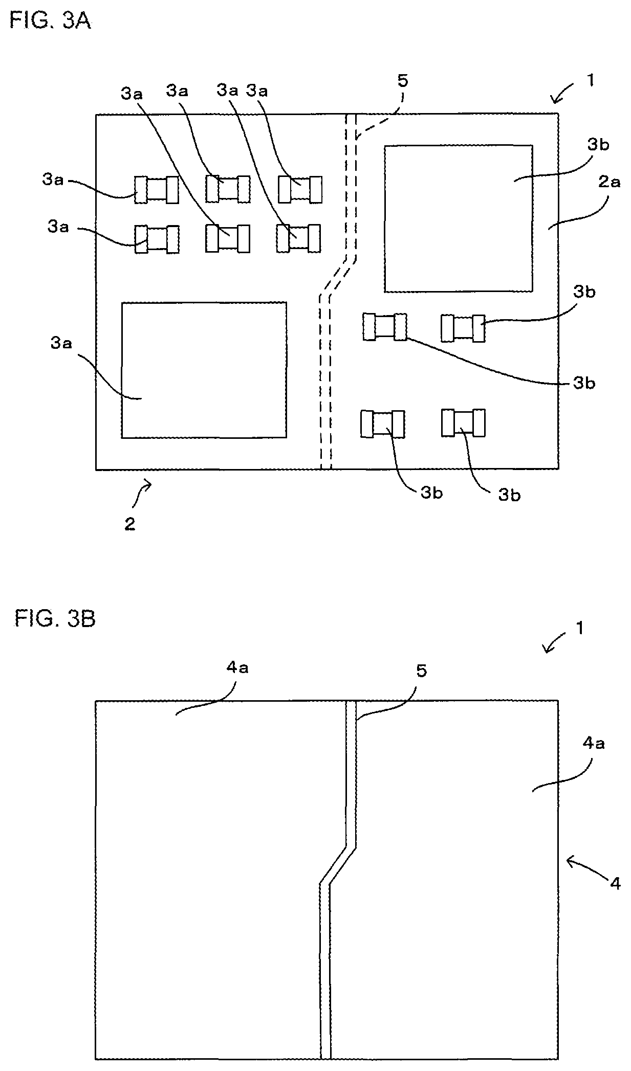
[0026]A module 1 according to a first embodiment of the present disclosure will be described with reference to FIGS. 1A through 7. FIGS. 1A and 1B illustrate perspective views of the module 1, where FIG. 1A is a perspective view of the top of the module 1 from an oblique direction, and FIG. 1B is a perspective view of the bottom of the module 1 from an oblique direction. FIG. 2 is a perspective view of the top of the module 1 illustrated in FIG. 1A, from an oblique direction, before the module is sealed with a resin. FIG. 3A is a plan view of the module 1 illustrated in FIG. 1A, before sealing with a resin, and FIG. 3B is a plan view of the module 1 illustrated in FIG. 1A, after the module is sealed with a resin and a trench is formed in the resin. Note that a first trench 5 illustrated in FIG. 3A is not actually present in the plan view of the module 1 before the module 1 is sealed with a resin, but is illustrated as an imaginary line for the sake of understanding, in order to clar...

second embodiment

[0051]A module according to a second embodiment of the present disclosure will be described with reference to FIGS. 8A through 10. Note that FIG. 8A is a plan view illustrating a module 1A according to the second embodiment, before the module 1A is sealed with a resin, and FIG. 8B is a bottom view of the module 1A, before the module 1A is sealed with a resin. Note that a first trench 5A illustrated in FIG. 8A is not actually present in the plan view of the module 1A before the module 1A is sealed with a resin, but is illustrated as an imaginary line for the sake of understanding, in order to clarify the positional relationship between the first trench 5A, and the first electronic components 3a and the second electronic components 3b, when viewed in plan view. Additionally, a second trench 11A illustrated in FIG. 8B is not actually present in the bottom view of the module 1A before the module 1A is sealed with a resin, but is illustrated as an imaginary line for the sake of understan...


PUM

PropertyMeasurementUnit
frequencyaaaaaaaaaa
temperatureaaaaaaaaaa
conductiveaaaaaaaaaa

Abstract

A first trench is formed in a first sealing resin layer, which seals first electronic components and second electronic components on one main surface of a circuit board, and a second trench is formed in a second sealing resin layer, which seals third electronic components and fourth electronic components on another main surface. The first trench is formed between the first electronic components and the second electronic components when viewed in plan view, extending from an upper surface of the first sealing resin layer toward a surface opposite from the one main surface of the first sealing resin layer, and the second trench is formed between the third electronic components and the fourth electronic components when viewed in plan view, extending from a lower surface of the second sealing resin layer toward a surface opposite from the other main surface of the second sealing resin layer.

Description

[0001]This is a continuation of International Application No. PCT / JP2017 / 043916 filed on Dec. 7, 2017 which claims priority from Japanese Patent Application No. 2016-242334 filed on Dec. 14, 2016. The contents of these applications are incorporated herein by reference in their entireties.BACKGROUNDTechnical Field[0002]The present disclosure relates to a module in which a trench is formed in a sealing resin layer that seals a component mounted on a circuit board.[0003]In a module where a plurality of electronic components such as semiconductor devices are mounted on a mounting surface of a circuit board, it is desirable that the level of integration of the electronic components be increased. However, as the level of integration of electronic components increases, there is a risk that unnecessary electromagnetic interference will arise among the electronic components. Thus, to suppress electromagnetic interference among electronic components in this type of module, covering the plural...

Claims


Application Information

Patent Timeline
Patent Type & Authority Patents(United States)
IPC IPC(8): H05K9/00H01L23/28H05K5/06H05K1/18H01L23/552H01L23/538H01L23/31H01L25/065H01L25/07H01L25/18H01L23/00H01L25/16
CPCH01L25/18H05K9/0037H01L25/065H05K5/065H01L25/07H05K1/181H01L23/00H01L23/552H05K5/064H05K9/0022H01L23/538H01L23/3121H01L23/28H01L25/16H05K2201/10522H05K2201/10545H01L2224/16227H01L2924/15313H01L2924/19041H01L2924/19042H01L2924/19043H01L2924/19105H01L2924/19106H01L2924/3025H01L24/16H05K9/0024H05K2201/09972H05K2203/1572H01L23/315H01L23/3135H01L23/04H01L25/0657H05K9/00
Inventor FURUYA, SHIN
Owner MURATA MFG CO LTD
Features
  • R&D
  • Intellectual Property
  • Life Sciences
  • Materials
  • Tech Scout
  • Unparalleled Data Quality
  • Higher Quality Content
  • 60% Fewer Hallucinations
Learn More