
Wearable electronic device and antenna system thereof

a wearable electronic device and wearable technology, applied in the field of wearable electronic devices, can solve the problems of poor isolation, reduced ground contact area of small-sized wearable electronic devices, and significant increase in the difficulty of full metal body design of antenna installation, etc., and achieve the effect of poor isolation

Active Publication Date: 2020-12-29
PEGATRON
View PDF13 Cites 1 Cited by
  • Summary
  • Abstract
  • Description
  • Claims
  • Application Information

AI Technical Summary

Benefits of technology

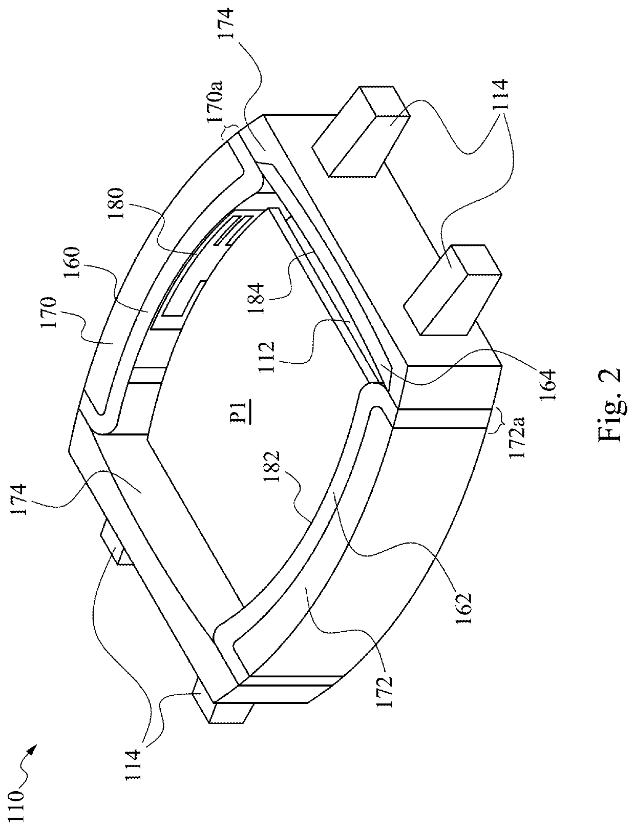
The present invention provides a solution for small wearable electronic devices with multiple antennas that can improve isolation between antennas and minimize the impact of the device's small interior space. The solution involves a middle frame, metallic side walls, and a first antenna wiring circuit. The first antenna pattern comprises a first metal portion and a second metal portion that generates a first resonant frequency band. The metallic side walls resonate with the first antenna pattern, allowing the antennas to be placed perpendicular to the device's bottom surface and utilize more interior space. This design allows for better sending and receiving efficiencies and qualities, even with the use of a full-metal body.

Problems solved by technology

However, smart equipment usually dispose antennas to provide wireless communication functions, and the full-metal body designs significantly increase the difficulty of antenna installation.
In addition, owing to the spatial constraint, the ground contact area of the small-sized wearable electronic devices is smaller.
If multiple antennas are intended to be disposed in the device, the antennas will interfere with one another, thus causing the problem of poor isolation.

Method used


Image

  • Wearable electronic device and antenna system thereof
  • Wearable electronic device and antenna system thereof
  • Wearable electronic device and antenna system thereof

Examples


Embodiment Construction

[0017]Reference will now be made in detail to the present embodiments of the disclosure, examples of which are illustrated in the accompanying drawings. Wherever possible, the same reference numbers are used in the drawings and the description to refer to the same or like parts.

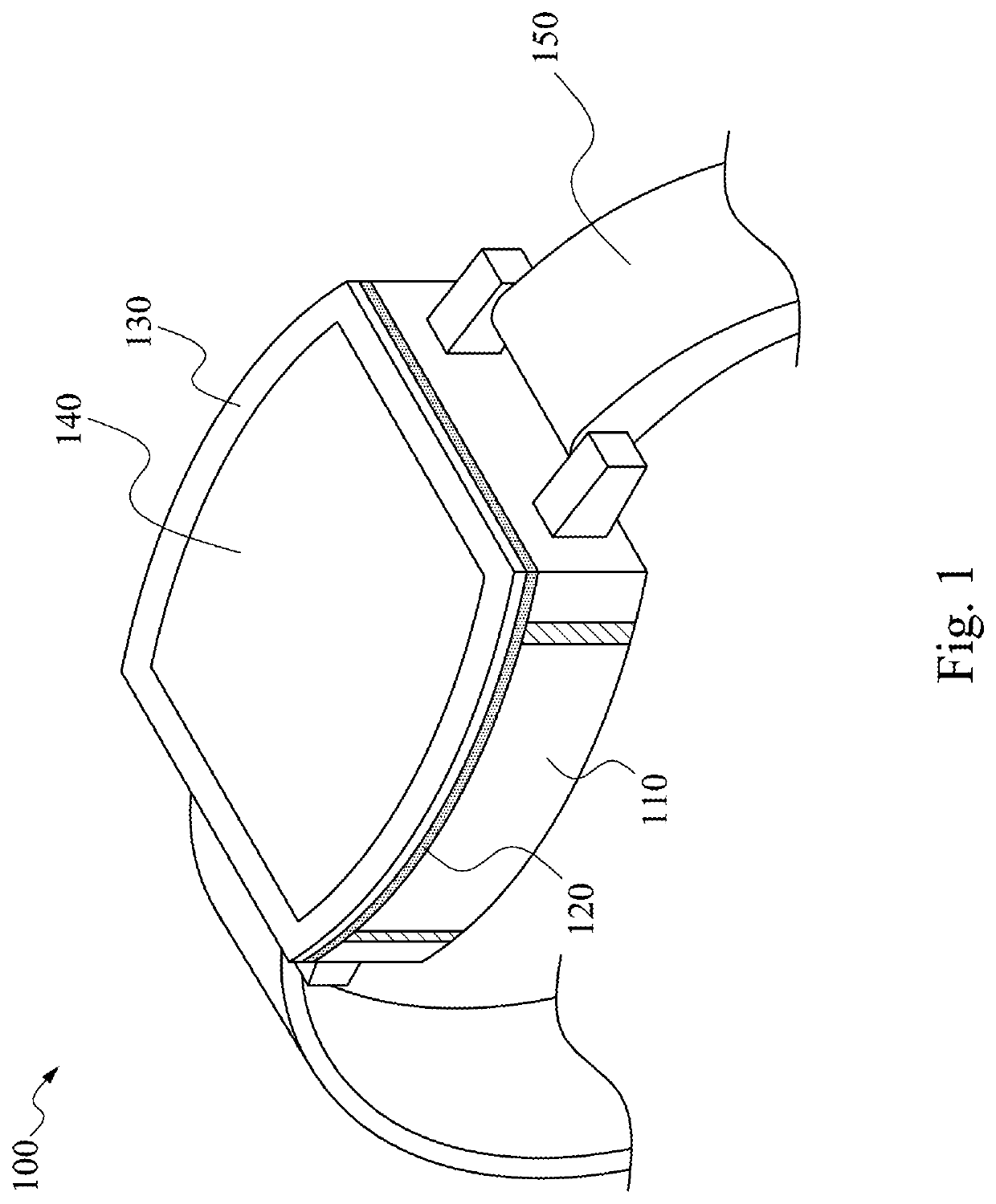
[0018]FIG. 1 depicts a schematic diagram of a wearable electronic device 100 according to one embodiment of the present disclosure. The wearable electronic device 100 is, for example, a watch. The wearable electronic device 100 has a middle frame 110, a dielectric bracing component 120, a bezel 130, a display panel 140, and a wearing component 150. The dielectric bracing component 120 may be plastic or any non-conductive material. The dielectric bracing component 120 is disposed at one side of the middle frame 110, that is, on the middle frame 110 and is configured to separate the middle frame 110 and the bezel 130. The bezel 130 is disposed at one side of the dielectric bracing component 120 opposite to the ...


PUM

PropertyMeasurementUnit
distanceaaaaaaaaaa
thicknessaaaaaaaaaa
Thicknessesaaaaaaaaaa

Abstract

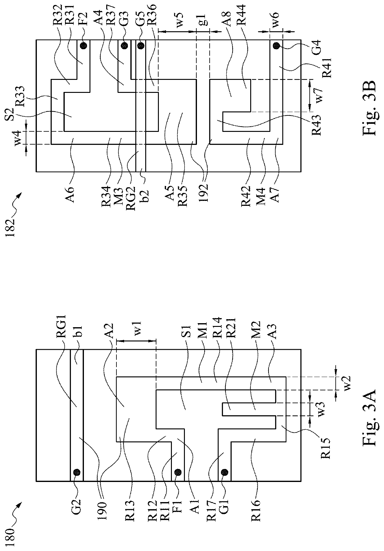
A wearable electronic device includes a middle frame, a metallic side wall, a dielectric element, and a antenna wiring circuit. The metallic side wall is disposed at one side of the middle frame and has a slot. The dielectric element is disposed at the slot and electrically isolates the metallic side wall and the middle frame. The antenna wiring circuit is disposed at the dielectric element and comprises a antenna pattern. The antenna pattern comprises first and second metal portions. The first metal portion comprises a slit surrounded by first to third segments. The first segment has a signal feeding terminal. The second metal portion is connected to the third segment and is located in the slit. The metallic side wall performs coupled resonant with the first metal portion and the second metal portion to generate a resonant frequency band.

Description

RELATED APPLICATIONS[0001]This application claims priority to Taiwan Application Serial Number 105136681, filed Nov. 10, 2016, which is herein incorporated by reference.BACKGROUNDField of Disclosure[0002]The present disclosure relates to a wearable electronic device. More particularly, the present disclosure relates to a wearable electronic device and an antenna system thereof having a communication function.Description of Related Art[0003]Small-sized wearable electronic devices, such as smart watches, smart bracelets, and the like, are becoming increasingly popular. In order to make the products more attractive, many manufacturers tend to use full-metal body designs. However, smart equipment usually dispose antennas to provide wireless communication functions, and the full-metal body designs significantly increase the difficulty of antenna installation. In addition, owing to the spatial constraint, the ground contact area of the small-sized wearable electronic devices is smaller. I...

Claims


Application Information

Patent Timeline
Patent Type & Authority Patents(United States)
IPC IPC(8): H01Q1/38H01Q1/24G04G21/04G04G17/02G01S19/24H01Q5/307H01Q1/27
CPCG01S19/24H01Q1/273H01Q1/38H01Q1/243G04G17/02H01Q5/307G04G21/04H01Q1/36H01Q1/44H01Q1/48
Inventor WU, CHIEN-YIKO, CHING-HSIANGWU, CHAO-HSUCHU, YU-YICHANG, CHIA-CHI
Owner PEGATRON
Learn More