Semiconductor device

a technology of semiconductor devices and semiconductors, applied in semiconductor devices, semiconductor/solid-state device details, electrical apparatus, etc., can solve the problems of deteriorating design freedom, increasing processing costs, and increasing production costs, so as to achieve production efficiency and design freedom. the effect of freedom

Active Publication Date: 2021-06-08
MITSUBISHI ELECTRIC CORP
View PDF5 Cites 0 Cited by
  • Summary
  • Abstract
  • Description
  • Claims
  • Application Information

AI Technical Summary

Benefits of technology

[0004]The present invention has been made to solve the above-described problems, and has an object to provide a semiconductor device capable of identifying a product without deteriorating production efficiency and degree of freedom in design.
[0006]In the present invention, the type of the product is exposed from the opening of the mounting board. Therefore, the type can be visually recognized without removing the mounting board. Furthermore, since the opening is originally provided to screw the semiconductor module to the heat radiation fin, it is not necessary to provide the mounting board with a dedicated opening only for visually recognizing the product model name. Therefore, the product can be identified without deteriorating the production efficiency and the degree of freedom in design.

Problems solved by technology

A dedicated opening may be provided in the mounting board so that the product model name is visually recognized, but this increases the processing cost.
Furthermore, since a place at which the product model name is printed varies according to each module, it is necessary to perform design of an opening for each module, which has caused a problem that the production efficiency deteriorates.
Furthermore, since it is impossible to provide a wiring pattern in the opening, there has also been a problem that the degree of freedom in design deteriorates.

Method used


Image

  • Semiconductor device
  • Semiconductor device
  • Semiconductor device

Examples


first embodiment

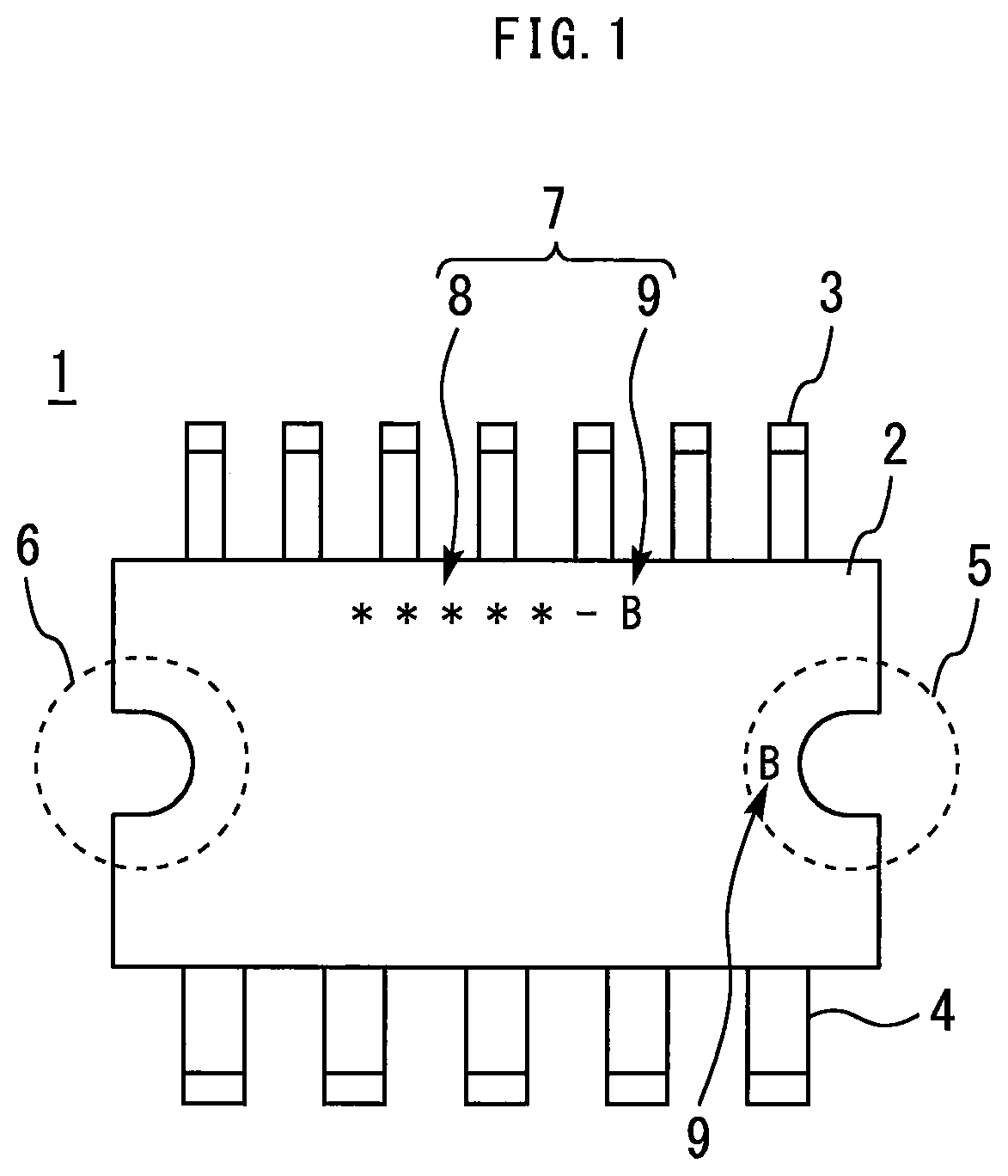
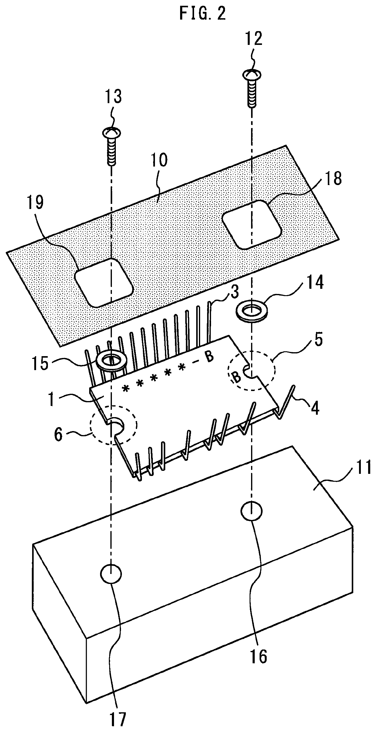
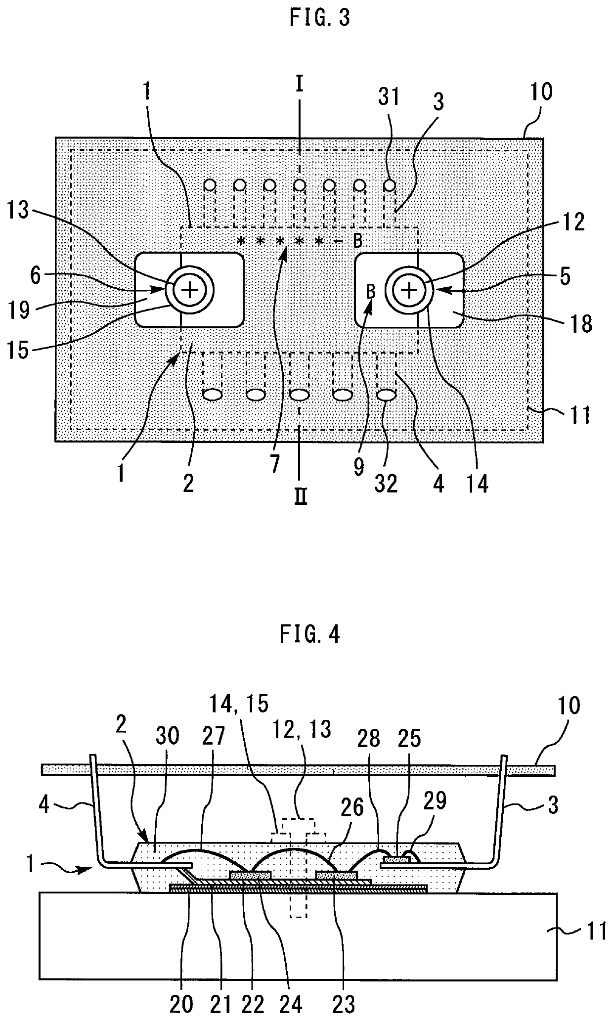
[0025]FIG. 1 is a top view illustrating a semiconductor module according to a first embodiment. The semiconductor module 1 has a transfer mold structure including a module main body 2, and terminals 3 and 4 protruding from side surfaces of the module main body 2 which are opposite to each other. The module main body 2 has first and second main surfaces which are opposite to each other. The first main surface is on this side of the drawing. The terminals 3 and 4 are bent toward the first main surface. Fitting portions 5 and 6 are provided at both ends in a longitudinal direction of the module main body 2 from which the terminals 3 and 4 do not project. The fitting portions 5 and 6 are provided with arc-shaped notches which allow screws to pass therethrough. A circular hole through which a screw passes may be provided instead of the notch.

[0026]A product model name 7 is printed on the first main surface of the module main body 2. The product model name 7 consists of a series name 8 an...

second embodiment

[0033]FIG. 5 is a top view illustrating a semiconductor device according to a second embodiment. A circle is printed as the type 9. Such a symbol is more easily analogized than a character even when only a part of the symbol is visually recognizable. Accordingly, a product can be identified when at least a part of the type 9 is printed outside the washers 14 and 15.

third embodiment

[0034]FIG. 6 is a top view illustrating a semiconductor device according to a third embodiment. The type 9 is printed on each of both the fitting portions 5 and 6, and exposed from at least one of the openings 18 and 19. Since the type 9 can be visually recognized through only one of the openings 18 and 19, the identification of the product is enhanced as compared with the second embodiment.


PUM

PropertyMeasurementUnit
diametersaaaaaaaaaa
diametersaaaaaaaaaa
degree of freedomaaaaaaaaaa

Abstract

A semiconductor device includes: a semiconductor module including a module main body having first and second main surfaces which are opposite to each other, and a terminal protruding from a side surface of the module main body and bent toward the first main surface; a mounting board placed on the first main surface side and connected to the terminal; a heat radiation fin placed on the second main surface side; and a screw fitting a fitting portion of the module main body from the first main surface side to the heat radiation fin, wherein the mounting board is provided with an opening at a portion facing the fitting portion, and a type of a product is printed on the first main surface and exposed from the opening of the mounting board.

Description

BACKGROUND OF THE INVENTIONField[0001]The present invention relates to a semiconductor device.Background[0002]With respect to a semiconductor module having a transfer mold structure, a mold name is printed on a mold surface (for example, see JP S62-014737 U). With respect to a power module, in order to improve the heat radiation of a power chip, a heat radiation fin having a size larger than a module size is mounted on a surface opposite to a mold surface which has been subjected to terminal bending. Therefore, a product model name is printed on the mold surface which has been subjected to terminal bending.SUMMARY[0003]Since a mounting board is mounted on the mold surface which has been subjected to terminal bending, it is necessary to remove the mounting board in order to confirm the model name after the mounting board has been mounted. A dedicated opening may be provided in the mounting board so that the product model name is visually recognized, but this increases the processing ...

Claims


Application Information

Patent Timeline
Patent Type & Authority Patents(United States)
IPC IPC(8): H01L23/367H01L23/40H01L23/00
CPCH01L23/3672H01L23/4006H01L24/45H01L2023/4087H01L23/13H01L23/544H01L23/367H01L2224/48137H01L2224/48245H01L2224/49109H01L2224/45124H01L2924/00014
Inventor SHIRAISHI, TAKUYA
Owner MITSUBISHI ELECTRIC CORP
Why Eureka
Try Eureka