Solid-state image pickup device with photoelectric charge transferrer to a floating diffusion region
a pickup device and photoelectric charge transfer technology, which is applied in the output circuit can solve the problems of reducing the gain of the source follower circuit, affecting the transmission efficiency of images, so as to reduce the power consumption of the solid-state image pickup device without deteriorating the conversion efficiency or frequency characteristic thereof.
- Summary
- Abstract
- Description
- Claims
- Application Information
AI Technical Summary
Benefits of technology
Problems solved by technology
Method used
Image
Examples
first circuit example
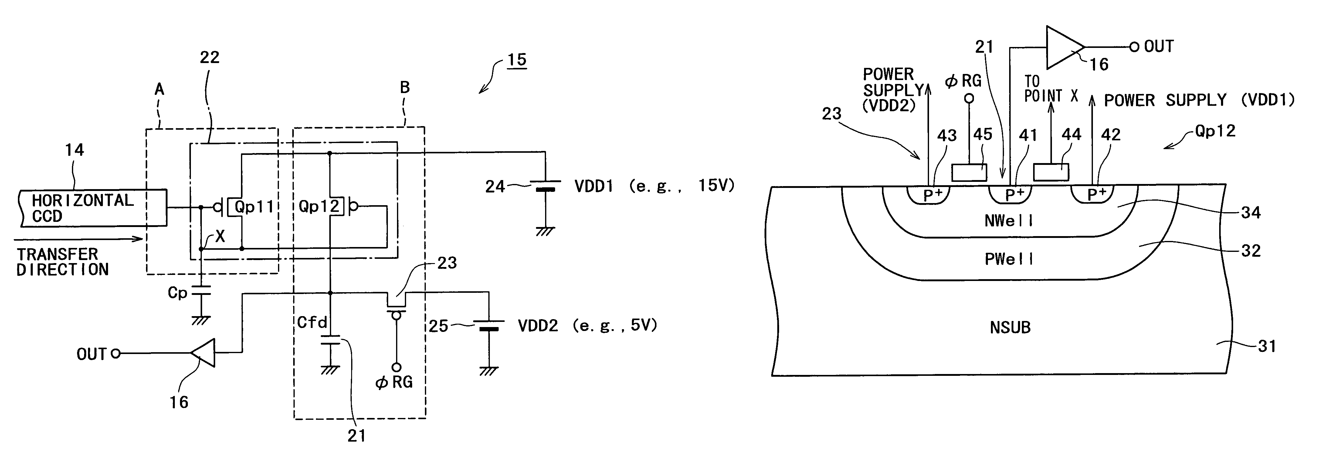
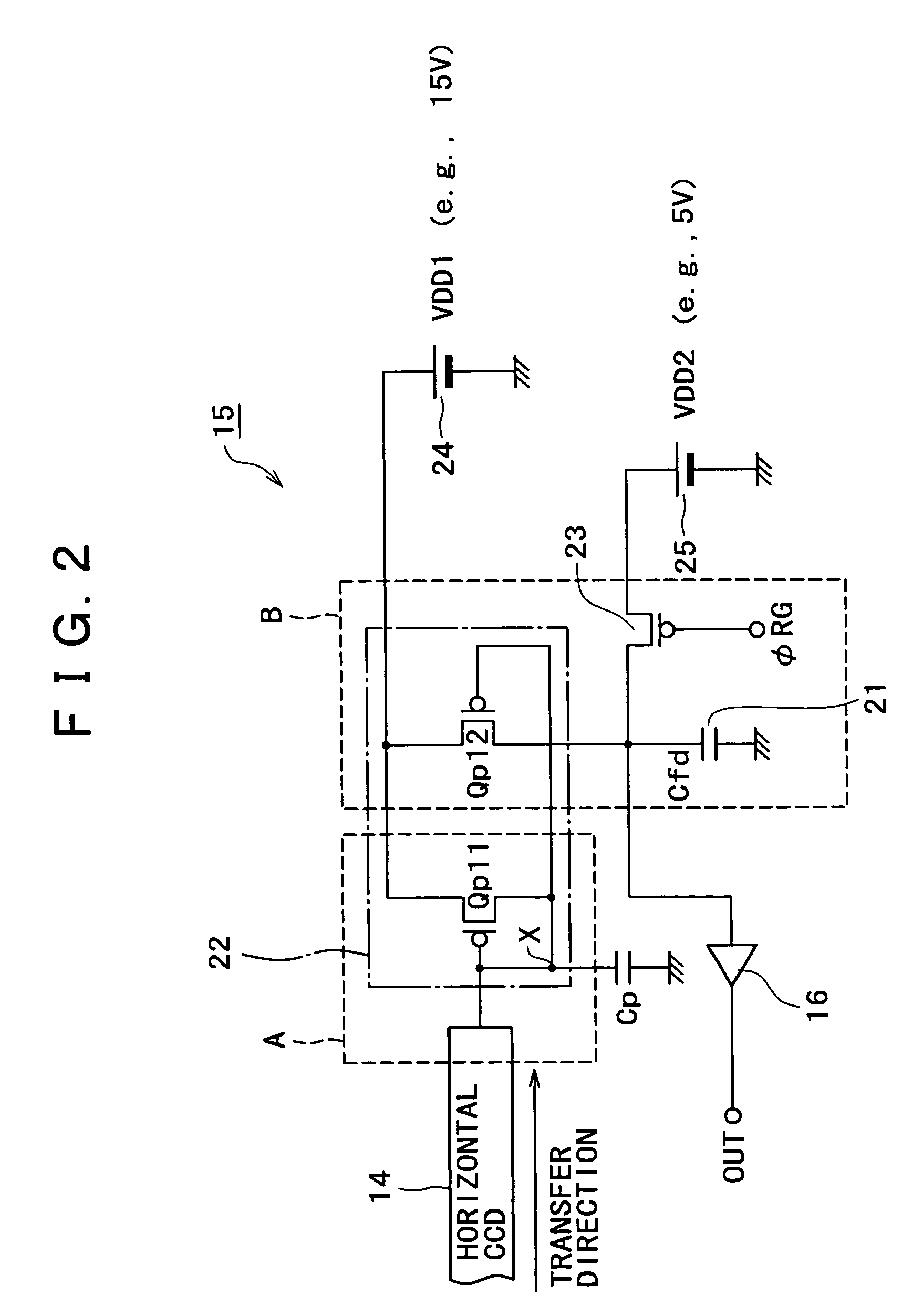
[0026]FIG. 2 is a circuit diagram showing a first circuit example with regard to the charge detector 15 and its peripheral portions. In FIG. 2, the charge detector 15 in this circuit example has a floating diffusion (FD) region 21; a current source such as, e.g., a current mirror circuit 22 for supplying the signal charge, which corresponds to the quantity of electric charge for the signal charge transferred by the horizontal CCD 14, to the floating diffusion region 21; and a reset transistor 23 for resetting the floating diffusion region 21.
[0027]The current mirror circuit 22 consists of a Pch MOS transistor Qp11 and a Pch MOS transistor Qp12. The gate and drain of the Pch MOS transistor Qp11 are connected in common to each other while being connected to one terminal of a parasitic capacitance Cp for temporarily storing the signal charge transferred by the horizontal CCD 14, and the source thereof is connected to the positive terminal of a DC power supply 24 for a first supply volt...
second circuit example
[0058]FIG. 7 is a circuit diagram showing a second circuit example with regard to a charge detector 15 and its peripheral portions. In this diagram, any component parts corresponding to those in FIG. 2 are denoted by like reference numerals or symbols.
[0059]In FIG. 7, a charge detector 15′ in this circuit example is so composed that a second current mirror circuit 26 is interposed between a current mirror circuit 22 and a floating diffusion region 21′, and a reset transistor 23′ consists of an Nch MOS transistor. Any other structure is the same as that of the charge detector 15 in the first circuit example.
[0060]The current mirror circuit 26 consists of an Nch MOS transistor Qn11 and an Nch MOS transistor Qn12. The gate and drain of the MOS transistor Qn11 are connected in common to the drain of a MOS transistor Qp12, and the source thereof is grounded. The gate of the MOS transistor Qn12 is connected in common to the gate of the MOS transistor Qn11, while the source thereof is grou...
PUM
 Abstract
Description
Claims
Application Information


