Power converter with over temperature protection compensation
a technology power converter, which is applied in the direction of power conversion systems, dc-dc conversion, instruments, etc., can solve the problems of increasing the risk of damage to the power converter, and increasing the risk of over temperature protection compensation
- Summary
- Abstract
- Description
- Claims
- Application Information
AI Technical Summary
Benefits of technology
Problems solved by technology
Method used
Image
Examples
first embodiment
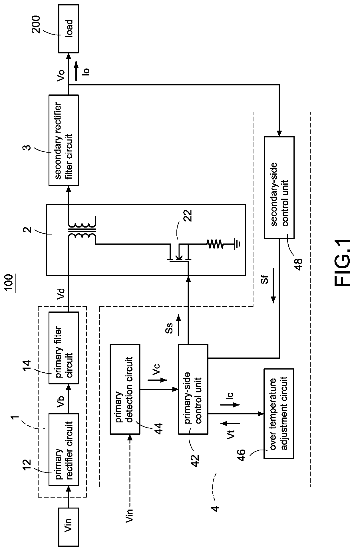
[0037]Please refer to FIG. 1, which shows a block circuit diagram of a power converter with over temperature protection compensation according to the present disclosure. The power converter 100 receives an input voltage Vin and converters the input voltage Vin into an output voltage Vo for supplying power to a load 200. The power converter 100 is a power converter 100 that accepts a wide input voltage Vin with an acceptable input voltage Vin ranging from 90 volts to 264 volts. The power converter 100 includes a primary rectifier filter circuit 1, a main conversion unit 2, a secondary rectifier filter circuit 3, and a control module 4. A primary side of the main conversion unit 2 is coupled to the primary rectifier filter circuit 1, and a secondary side of the main conversion unit 2 is coupled to the secondary rectifier filter circuit 3. The control module 4 controls the main conversion unit 2 to convert the input voltage Vin into the output voltage Vo through a path composed of the ...
second embodiment
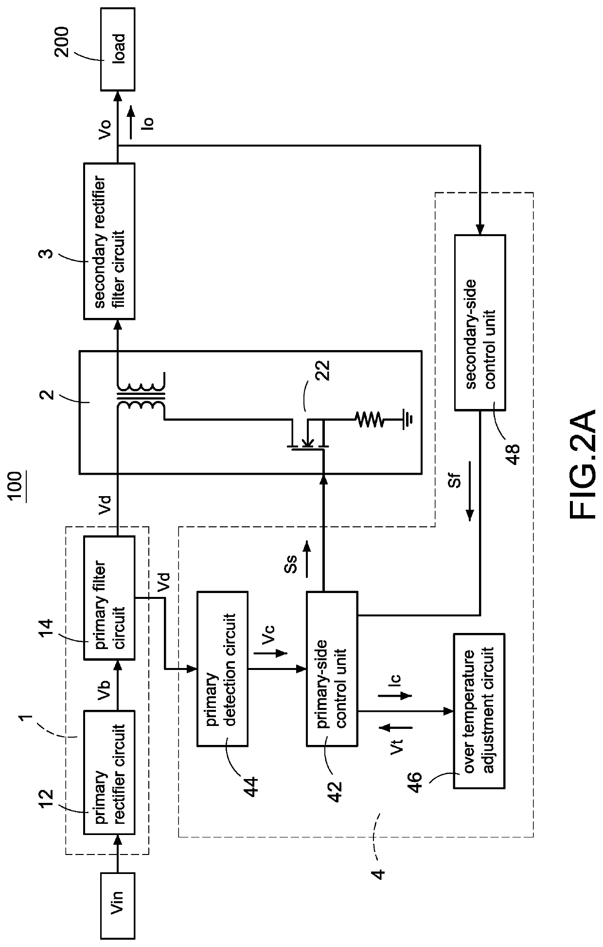
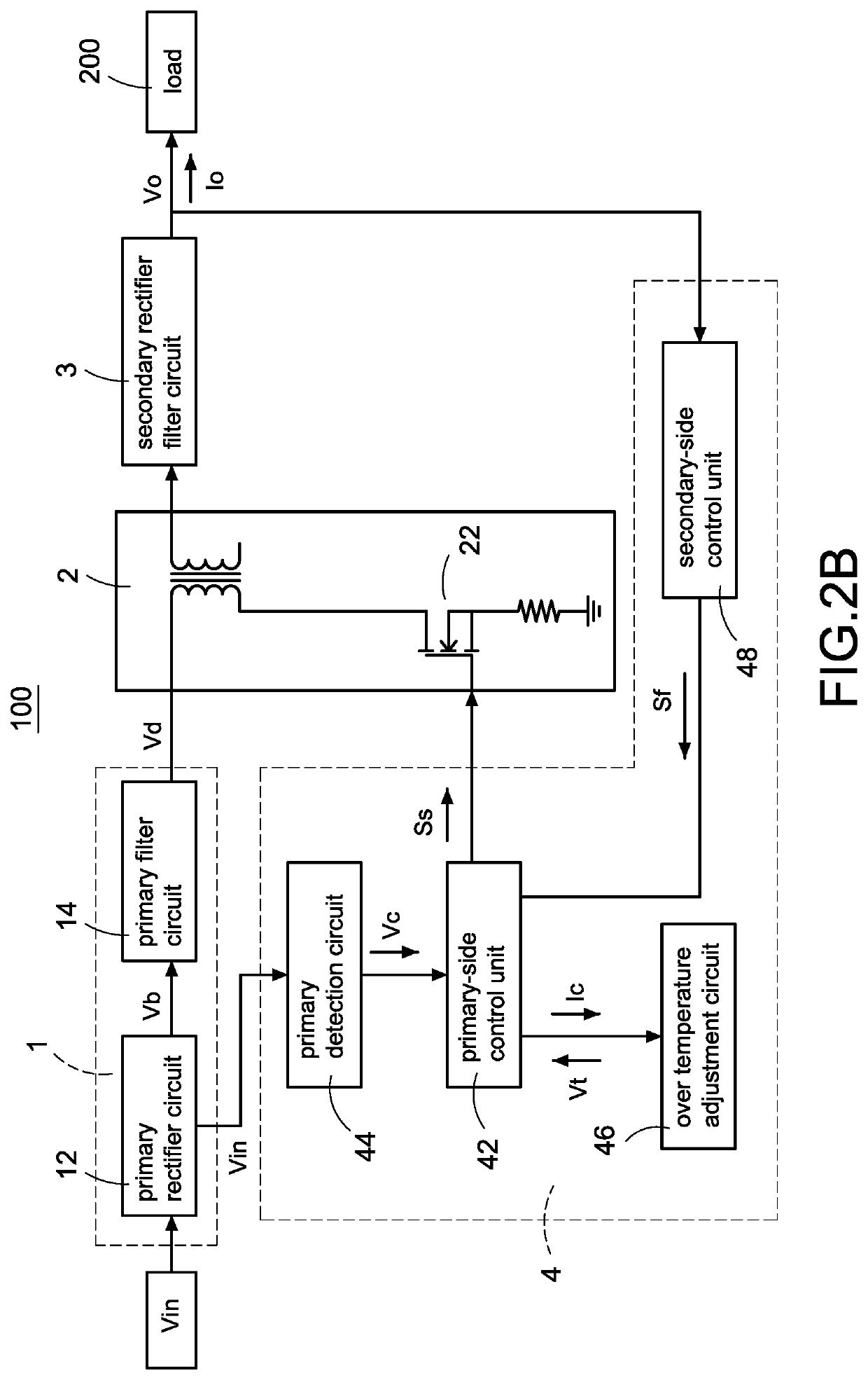
[0055]In one embodiment, the temperature compensation circuit 462 is not limited to the coupling manner as shown in FIG. 5, and may be coupled between the primary-side control unit 42′ and the temperature control resistor Rt, or between the temperature control resistor Rt and the ground point. In one embodiment, the unexplained circuit structure and control manner of the power converter 100′ according to FIG. 5 are the same as those of FIG. 1. The detection manner applicable to the primary voltage change value Vc of FIG. 2A to FIG. 2D and the internal structure of the primary detection circuit 44 are also applicable to the circuit structures of FIG. 3A to FIG. 3B, and will not be described again here.
[0056]Please refer to FIG. 6, which shows a block circuit diagram of a temperature compensation circuit according to the present disclosure, and also refer to FIG. 1 to FIG. 5. The temperature compensation circuit 462 includes a detection circuit 462A, a voltage control switch 462B, a c...
PUM
 Abstract
Description
Claims
Application Information


